EN
EN
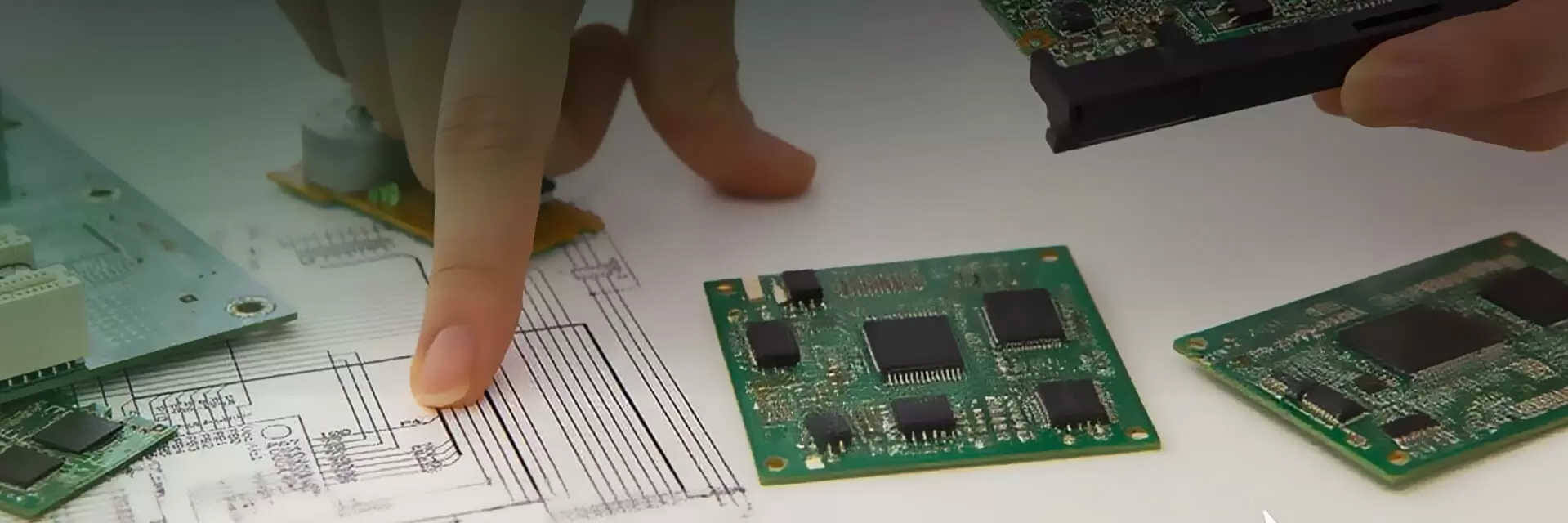
Development and Solutions
For any inquiries, please contact us. We are dedicated to providing you with the highest quality service.-BBBBB
 Home > Development and Solutions
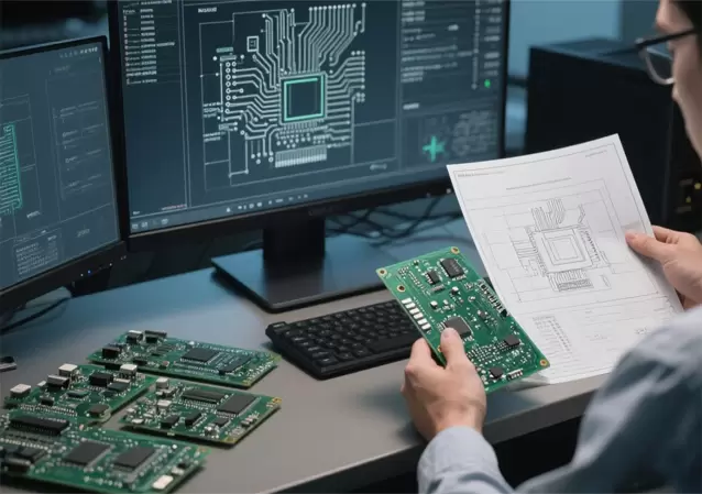
 Design Concept Development, Block Diagram, Power Estimation
Schematic Capture, BOM Cost Estimation
Enclosure/Chassis Design
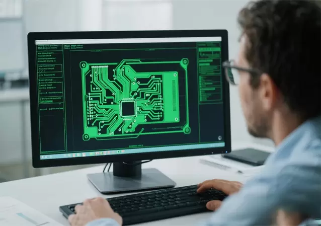
PCB Layout Research
PCB Layout Design
Thermal/Power Simulation
Power Integrity and Signal Integrity Analysis
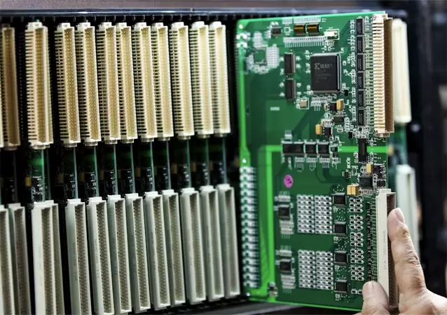
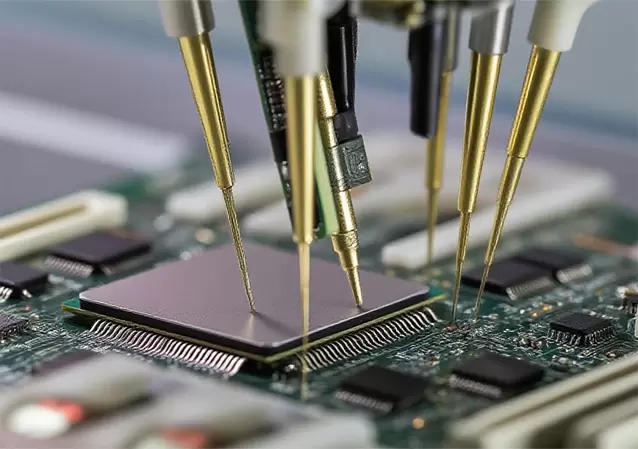
PCB Manufacturing and Assembly
Board Debugging and Testing
Hardware User Manual, Application Notes
System and Board-Level Architecture Specifications
Engineering Design Specifications
Component Selection
Component Obsolescence and Planning
Symbol Creation
Schematic/Capture
Timing Analysis
Netlist Generation
BOM Generation
Tools: (OrCAD, Concept HDL, Altium, PAD, Expedition)