The IC substrate sits between the silicon die and the main PCB, handling fine-pitch interconnections that standard boards cannot support. As packaging density increases, this layer becomes critical for maintaining stable signal transmission and reliable power distribution.
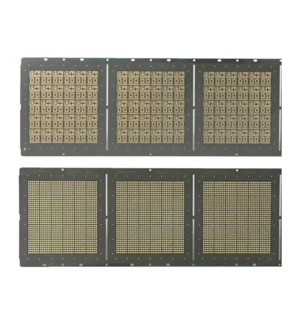
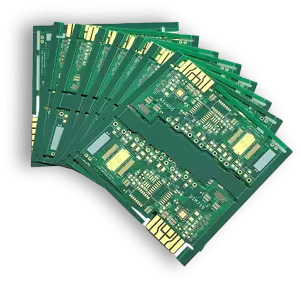
Most IC substrates are developed for specific projects rather than produced as standard items. The design is usually defined by chip layout, package structure, and performance targets. Line width, layer count, and via configuration are all adjusted to match the routing complexity of the device.
Structure and Key Specifications
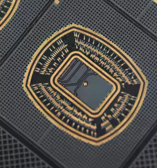
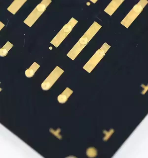
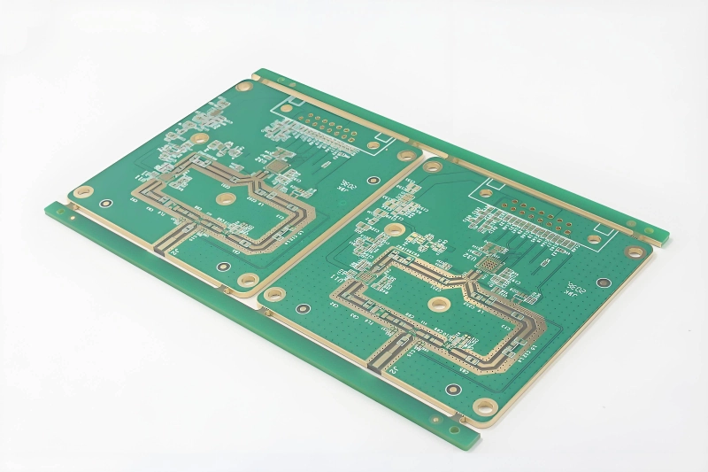
IC substrates are built with high-density interconnect structures. Fine lines, microvias, and multi-layer build-up processes are used to route signals within a very limited space. As designs become more complex, layer counts increase, and so does the need for tighter alignment control.
Copper thickness is selected based on circuit function. Thin copper supports dense signal routing, while thicker copper is used in areas that carry higher current. Surface finishing is chosen to match assembly requirements and ensure consistent soldering performance.
The combination of layer structure, via design, and material selection directly affects electrical stability and assembly accuracy.
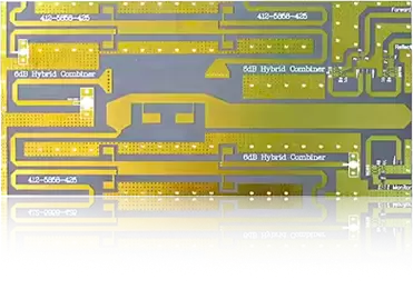
Application-Driven Design
IC substrate design changes depending on where it is used.
High-performance computing and communication equipment require stable signal transmission under high-speed conditions. Automotive electronics place more emphasis on long-term reliability and resistance to temperature variation. Consumer devices focus on reducing size while maintaining functionality.
These differences mean that IC substrates are rarely interchangeable. Each design is built around the conditions it will operate in, not just a general specification.
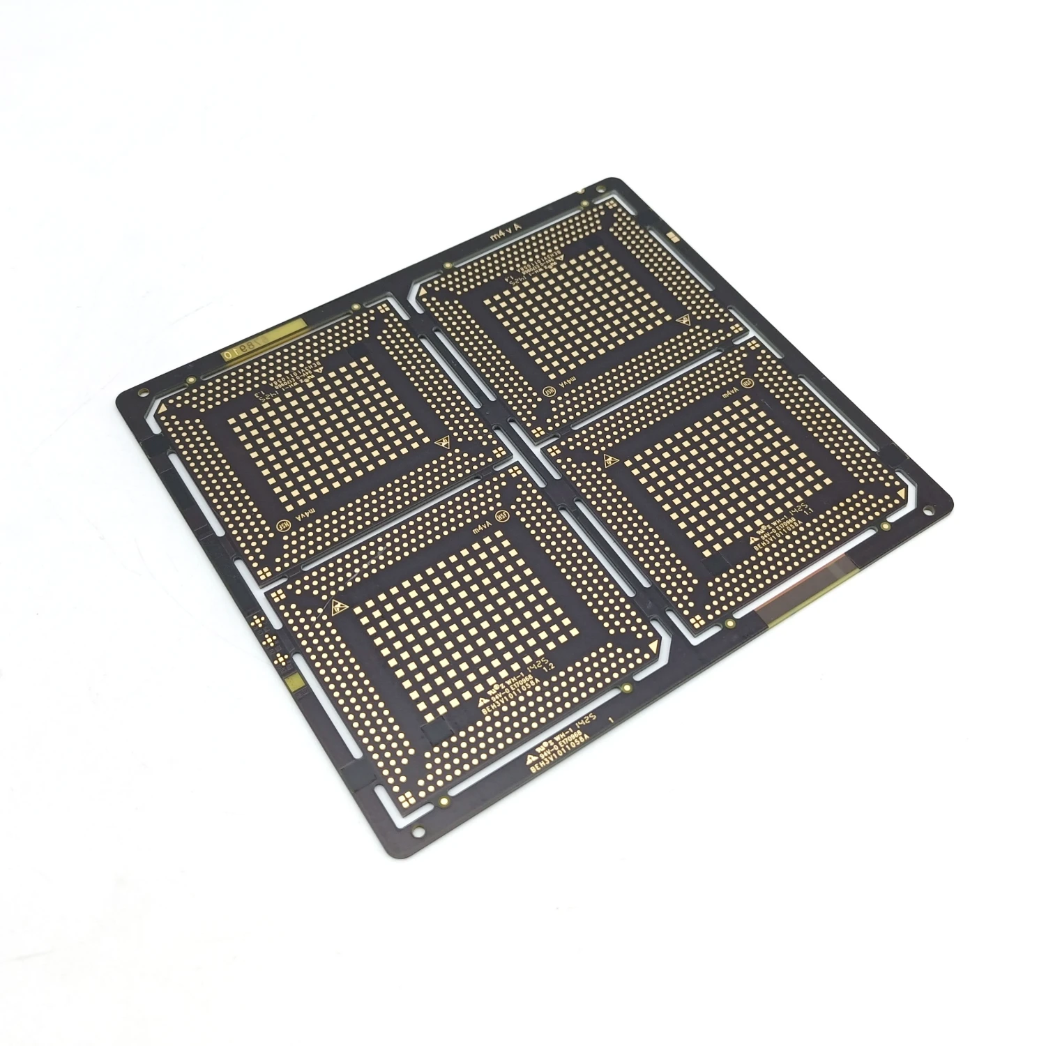
Manufacturing and Reliability
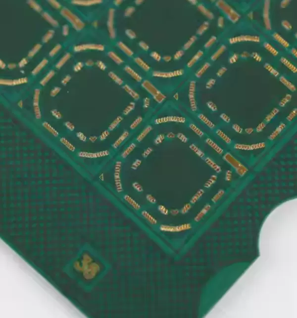
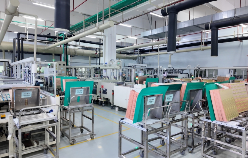
Producing IC substrates involves tight control across multiple process steps. As line width decreases and layer count increases, small variations can affect both yield and performance.
Key factors include microvia formation, layer alignment, and control of board warpage during lamination. These directly influence how well the substrate performs during assembly and in actual use.
Before delivery, substrates go through electrical testing and structural inspection to confirm connectivity and internal quality. In many applications, they also need to remain stable under temperature cycling and long operating hours, making reliability a central requirement.
 en
en

 WhatsApp