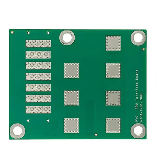
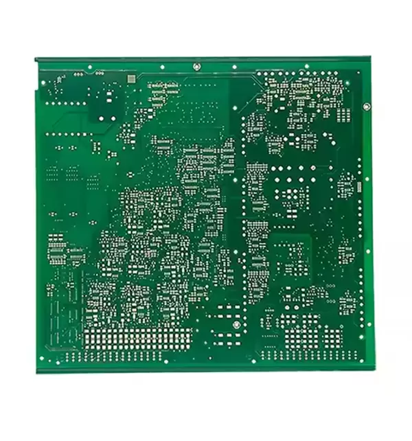
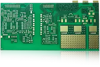
Multi-layer PCB for High-Density, High-Speed Electronic Applications
When circuit complexity starts pushing beyond the limits of 2-layer or 4-layer designs, a well-built Multi-layer PCB becomes the only practical solution. Instead of forcing compromises in routing or board size, multi-layer structures open up vertical space, allowing engineers to integrate dense circuitry without sacrificing performance or reliability.
In real projects, this matters most where space is fixed, but functionality keeps growing—AI computing boards, industrial control units, medical electronics, and communication systems. A properly designed multi-layer structure doesn’t just “add layers”; it reorganizes how signals, power, and grounding interact across the board.
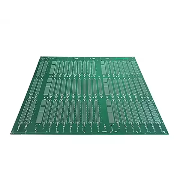
High-Density Layout Without Sacrificing Stability
One of the biggest challenges in modern electronics is fitting more into less space. A Multi-layer PCB addresses this by distributing routing across multiple internal layers, reducing congestion on outer layers, and making complex layouts manageable.
Instead of forcing tight traces and risky routing decisions, engineers gain flexibility:
- Signal layers can be separated from power layers to reduce interference
- Ground planes can be positioned to stabilize return paths
- Critical signals can be routed with more controlled geometry
This approach is especially useful in compact devices where board size cannot increase, but performance demands continue to rise. The result is not just higher density, but a cleaner and more predictable layout.
Reliable Signal Integrity for High-Speed Circuits
As data rates increase, signal behavior becomes far less forgiving. In high-speed designs, a Multi-layer PCB plays a direct role in maintaining signal integrity.
Controlled impedance is not just a specification—it’s what keeps interfaces like DDR, PCIe, and high-frequency communication links functioning correctly. By carefully managing layer stack-up and trace geometry, signal paths remain consistent, reducing reflections, loss, and crosstalk.
More importantly, multi-layer structures allow:
- Dedicated reference planes for stable impedance
- Shorter and more direct signal paths
- Better isolation between high-speed and noisy circuits
In practice, this means fewer signal issues during testing and more predictable performance once the product is deployed.
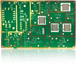
Thermal and Power Performance That Holds Up in Real Use
In many applications, heat and current handling are where standard boards begin to struggle. A Multi-layer PCB offers more than just routing space—it creates opportunities to manage power distribution and heat dissipation more effectively.
With proper design:
- Thicker copper layers can be used for high-current paths
- Internal planes help distribute heat more evenly
- Power layers reduce voltage drop across the board
This becomes critical in systems that run continuously or operate under load, such as industrial equipment, power electronics, and embedded control systems. Instead of localized overheating or unstable power delivery, the board maintains consistent performance over time.
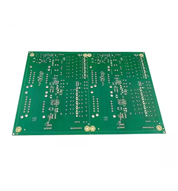
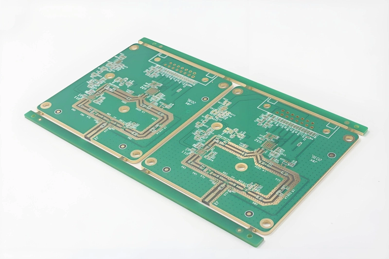
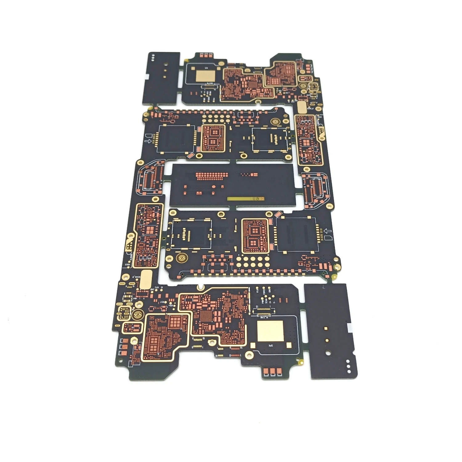
Stack-up Design That Matches the Application, Not Just the Drawing
Not all multi-layer boards are built the same. The real difference often lies in how the layers are arranged.
A well-planned Multi-layer PCB stack-up considers:
- Signal priority and routing paths
- Power distribution requirements
- Grounding strategy for noise control
- Mechanical balance to prevent warping
Rather than simply following a fixed structure, stack-up design should reflect the needs of the application. High-speed boards, for example, require tighter control of impedance and layer symmetry, while power-focused designs may prioritize copper thickness and thermal paths.
This is where engineering input matters. Adjusting the stack-up early can prevent signal issues, reduce EMI risks, and improve overall manufacturability.
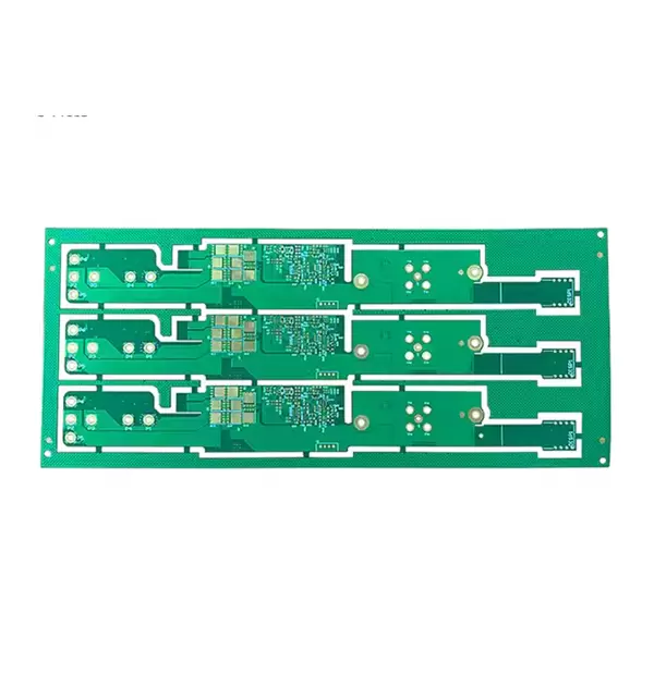
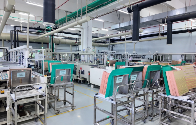
From Prototype to Production with Consistent Results
Getting a prototype to work is one thing. Producing it consistently at scale is another.
A reliable Multi-layer PCB supplier needs to support both stages without introducing variability. That includes:
- Fast turnaround for prototype builds
- Stable process control during batch production
- Consistent material sourcing and layer alignment
- Engineering checks before manufacturing begins
For customers, this reduces the risk of redesigns, delays, or unexpected performance shifts between prototype and mass production. It also shortens the path from development to market.
Manufacturing Capability Overview
- Layer count: 4 to 50+ layers
- Board thickness: customizable (standard 1.6mm and above)
- Base material: FR-4 and advanced material options available
- Copper thickness: 0.5oz to 5oz
- Minimum hole size: 0.1mm
- Minimum line width/spacing: 0.075mm
- Surface finishing: Lead-Free HASL, OSP, and more
- Service: OEM, custom packaging, and project-based support
These specifications support a wide range of applications, from standard industrial boards to more complex high-density designs.
Why Multi-layer PCB Is the Right Choice for Complex Electronics
For projects where space, speed, and stability all matter, a Multi-layer PCB is no longer optional. It provides a structured way to handle complexity—organizing signals, power, and thermal performance into a single, reliable platform.
The advantage is not just in the number of layers, but in how those layers are used. When designed and manufactured correctly, multi-layer boards support long-term performance, reduce design limitations, and make advanced electronic systems possible.
 en
en

 WhatsApp