DIP
DIP
One-stop SMT assembly
Our factories provide high -quality SMT assembly services for medical, aerospace, national defense industry, automobiles, communications and consumer electronics.

homeHome > PCB Assembly > DIP&Wave-Soldering Introduction

DIP&Wave-Soldering Introduction

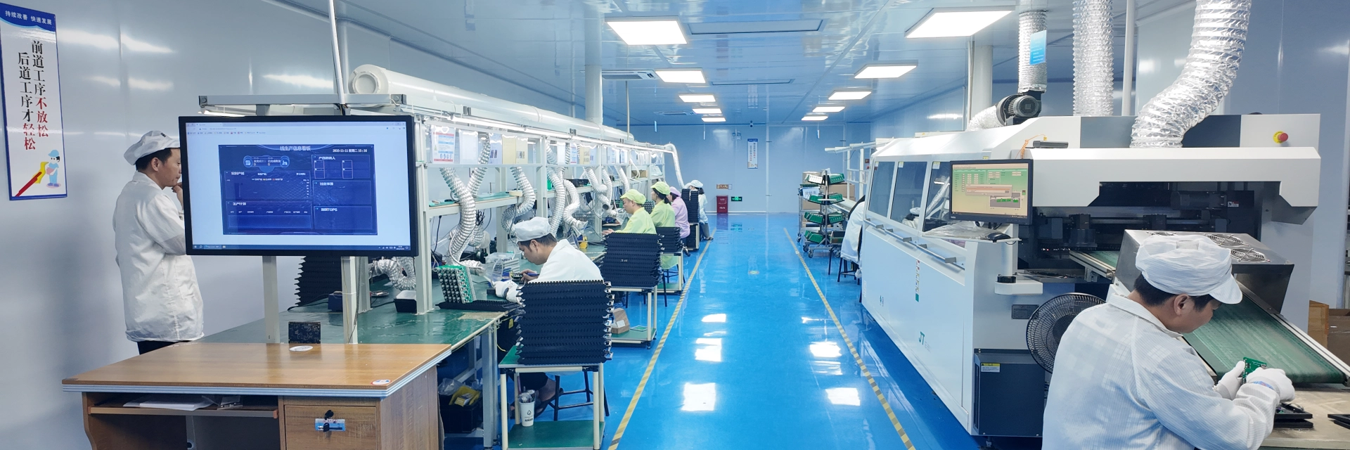
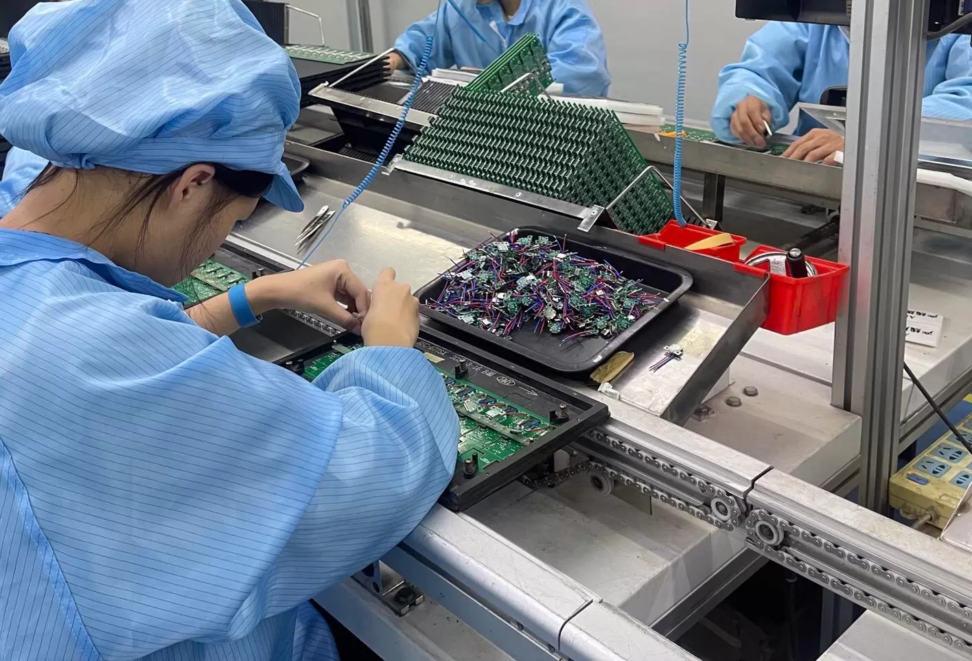
DIP (Dual In-line Package) and wave soldering are essential processes in through-hole PCB assembly. DIP refers to electronic components with two parallel rows of pins, which are inserted into pre-drilled holes on the PCB. These components are widely used for ICs, resistors, capacitors, and connectors that require strong mechanical stability.


Wave soldering is a high-efficiency soldering method used to attach these through-hole components. During the process, the PCB passes over a wave of molten solder, simultaneously soldering all component pins. Preheating and flux application ensure strong, reliable solder joints and prevent defects like solder bridges or cold joints.


Together, DIP insertion and wave soldering provide a robust and efficient solution for through-hole PCB assembly, balancing production speed with high reliability.


SMT Assembly Process Step

Solder Paste Application
Stencil printing deposits precise amounts of solder paste onto designated PCB contact pads.
01
Component Placement
Automated pick-and-place machines retrieve surface-mount devices (SMDs) and accurately position them onto the solder paste-coated pads.
02
Reflow Soldering:
Boards pass through a controlled thermal oven, melting the solder paste to form permanent electrical and mechanical connections.
03
Automated Optical Inspection (AOI):
Vision systems verify component presence, placement accuracy, polarity, and basic solder joint quality post-reflow.
04
Through-Hole Component Insertion
Remaining non-SMD parts (connectors, large capacitors) are manually or automatically inserted into plated through-holes.
05
Wave Soldering (For Mixed Technology):
Boards with through-hole components pass over a molten solder wave, forming connections on the underside.
06
Conformal Coating (If Required):
Protective chemical layer applied to shield assembled boards from environmental factors (moisture, dust, chemicals).
07
Secondary Reflow (For Double-Sided Assembly):
Process repeats (steps 1-4) for components on the board's opposite side, using higher-temperature solder or adhesive.
08
Advanced Inspection & Testing:

X-ray Inspection (AXI): Examines hidden connections (BGAs, QFNs) for voids, bridging, or alignment defects.

In-Circuit Testing (ICT): Electrical verification of component functionality and circuit performance.

Functional Testing (FCT): Validates the fully assembled board against operational specifications.

09
Cleaning & Final Assembly:
Flux residues removed (if needed); boards undergo final integration (housing, connectors) in a controlled environment.
10
Rework & Repair:
Dedicated stations (BGA rework, SMT IR) correct identified defects for component replacement or solder joint remediation.
11