DIP
DIP
One-stop SMT assembly
Our factories provide high -quality SMT assembly services for medical, aerospace, national defense industry, automobiles, communications and consumer electronics.

homeHome > PCB Assembly > DIP&Wave-Soldering

DIP&Wave-Soldering
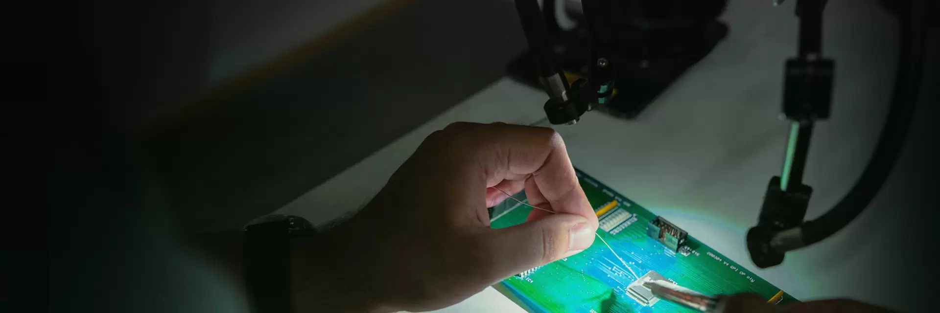
Surface Mount Technology (SMT) is a methodology for mounting electronic components directly onto the surface of a Printed Circuit Board (PCB). This process utilizes robotic systems to precisely position miniature components onto designated PCB pads. Assembly is finalized through reflow soldering or wave soldering techniques. SMT offers advanced automation and exceptional precision, significantly boosting manufacturing efficiency while minimizing human error, making it the dominant solution in contemporary electronics production.
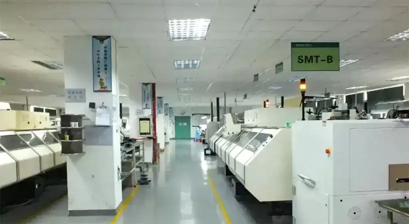
Our facility boasts cutting-edge manufacturing infrastructure and sophisticated machinery to ensure superior fabrication. We employ highly skilled and seasoned specialists dedicated to delivering rapid turnaround times without compromising on quality. Our comprehensive capabilities in premium SMT PCB assembly services encompass:
A state-of-the-art prototype SMT line enabling swift and adaptable manufacturing.
Dedicated stations for BGA removal/replacement, SMT infrared (IR) rework, and through-hole component rework.
An extensive component library stocked with production-ready parts to accelerate build cycles.
A meticulously clean, organized, and secure setting for final assembly operations.
Advanced equipment delivering unmatched technical performance and product integrity.
Rigorous inspection and testing utilizing X-ray analysis, Automated Optical Inspection (AOI), and microscopy up to 20X magnification.
DIP&Wave-Soldering Assembly Process Step
Solder Paste Application
Stencil printing deposits precise amounts of solder paste onto designated PCB contact pads.
01
Component Placement
Automated pick-and-place machines retrieve surface-mount devices (SMDs) and accurately position them onto the solder paste-coated pads.
02
Reflow Soldering:
Boards pass through a controlled thermal oven, melting the solder paste to form permanent electrical and mechanical connections.
03
Automated Optical Inspection (AOI):
Vision systems verify component presence, placement accuracy, polarity, and basic solder joint quality post-reflow.
04
Through-Hole Component Insertion
Remaining non-SMD parts (connectors, large capacitors) are manually or automatically inserted into plated through-holes.
05
Wave Soldering (For Mixed Technology):
Boards with through-hole components pass over a molten solder wave, forming connections on the underside.
06
Conformal Coating (If Required):
Protective chemical layer applied to shield assembled boards from environmental factors (moisture, dust, chemicals).
07
Secondary Reflow (For Double-Sided Assembly):
Process repeats (steps 1-4) for components on the board's opposite side, using higher-temperature solder or adhesive.
08
Advanced Inspection & Testing:

X-ray Inspection (AXI): Examines hidden connections (BGAs, QFNs) for voids, bridging, or alignment defects.

In-Circuit Testing (ICT): Electrical verification of component functionality and circuit performance.

Functional Testing (FCT): Validates the fully assembled board against operational specifications.

09
Cleaning & Final Assembly:
Flux residues removed (if needed); boards undergo final integration (housing, connectors) in a controlled environment.
10
Rework & Repair:
Dedicated stations (BGA rework, SMT IR) correct identified defects for component replacement or solder joint remediation.
11