 en
en
 Home > PCB Fabrication > Preparation and Cutting > New Energy Charger PCB Assembly
New Energy Charger PCB Assembly
Case Study: New Energy Charger PCB Assembly — Powering Efficient, Safe EV Charging Infrastructure
In the rapidly expanding new energy sector, reliable charging infrastructure is the backbone of electric vehicle (EV) adoption. A leading manufacturer of EV charging solutions approached us to address critical challenges in assembling PCBs for their next-gen 60kW DC fast chargers. The project demanded a balance of high-power handling, thermal resilience, and strict safety compliance—key pillars of new energy charger performance.
Project Background & Client Requirements
The client’s 60kW DC charger targets commercial and public charging stations, requiring PCBs that could:
· Handle high currents (up to 150A) and voltages (800V DC) without degradation.
· Operate in harsh outdoor environments (-30°C to 60°C) with resistance to humidity, dust, and corrosion.
· Support fast charging protocols (CCS, CHAdeMO) with stable communication between the charger and EV.
· Meet stringent safety standards (UL 60950, IEC 61851) to prevent overheating, short circuits, or electric shock.
· Scale from prototype (50 units) to mass production (5,000 units/month) with consistent quality (PPM ≤20).
Key Challenges in New Energy Charger PCB Assembly
The project posed unique hurdles tied to the high-power, high-voltage nature of EV charging:
1. Thermal Management Under Load: Power conversion components (IGBTs, rectifiers) generate extreme heat during fast charging, risking solder joint fatigue or component failure.
2. High-Voltage Insulation: PCB traces and components must withstand 800V DC with strict creepage (≥8mm) and clearance (≥6mm) distances to prevent arcing.
3. Signal Integrity in Noisy Environments: Communication modules (e.g., CAN, Ethernet) are vulnerable to electromagnetic interference (EMI) from high-power circuits, threatening charging protocol reliability.
4. Material Durability: Outdoor deployment requires PCBs resistant to UV radiation, moisture, and chemical exposure (e.g., road salts).
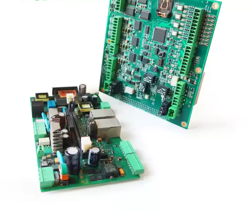
Our Tailored Assembly Solutions
To overcome these challenges, we designed a holistic assembly strategy focusing on power handling, thermal resilience, and safety compliance:
1. PCB Design & Material Engineering
· Substrate Selection: Used 4-layer PCBs with high-Tg (180°C) FR-4 material and 2oz copper cladding to enhance current-carrying capacity and heat dissipation.
· Thermal Path Optimization: Integrated thermal vias (diameter 0.3mm) beneath power components to transfer heat from the PCB to an external heatsink, reducing operating temperatures by 25°C under full load.
· High-Voltage Layout: Segregated high-voltage (power stage) and low-voltage (control/communication) zones with grounded isolation barriers, ensuring creepage/clearance compliance.
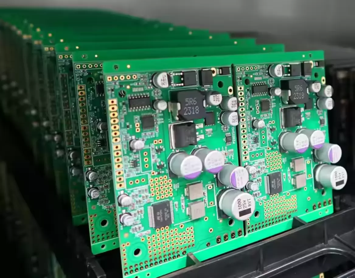
2. Precision Assembly for High-Power Components
SMT for Control & Communication Circuits:
· Deployed DEK NeoHorizon printers with laser-aligned stencils to apply solder paste accurately on fine-pitch components (e.g., 0.5mm BGA for the main controller).
· Used Fuji NXT III pick-and-place machines (accuracy ±15μm) to place SMD components, including temperature sensors and communication ICs, with minimal positional error.
Power Component Assembly:
· Employed selective wave soldering for through-hole power connectors (rated 200A), ensuring robust joints capable of handling high current.
· For IGBT modules (critical to power conversion), used eutectic solder (Sn95Pb5) with a controlled reflow profile (peak 230°C) to achieve void-free bonds (<3% void rate) and maximize thermal conductivity.
3. Rigorous Testing & Compliance Validation
·
Electrical Safety Testing:
· Hipot testing at 3kV AC for 1 minute to verify insulation integrity between high- and low-voltage zones.
· Ground continuity tests (<0.1Ω resistance) to ensure safe fault current dissipation.
Performance & Reliability Validation:
· Power cycling tests (1,000 cycles from 10% to 100% load) to simulate real-world charging patterns, monitoring for voltage drop or temperature spikes.
· Environmental chamber testing: 500 hours at 95% humidity (40°C) to validate resistance to moisture, followed by thermal shock tests (-30°C to 60°C, 100 cycles).
Protocol Compliance:
· Verified communication stability via signal integrity testing (eye diagram analysis for CAN bus signals) to ensure error-free interaction with EVs.
Project Outcomes & Client Impact
· Performance Metrics: The assembled PCBs enabled the charger to deliver 60kW power with 96.5% efficiency, maintaining stable operation even at 60°C ambient temperature.
· Safety Compliance: Passed UL 60950 and IEC 61851 certifications on the first attempt, accelerating the client’s market launch by 8 weeks.
· Scalability: Streamlined processes allowed us to ramp up production from 50 prototypes to 5,000 units/month within 6 weeks, with a consistent yield of 99.1%.
· Cost Efficiency: Optimized material selection (e.g., high-performance yet cost-effective FR-4) and automated testing reduced per-unit assembly costs by 12%.
Why Partner With Us for New Energy Charger PCBs?
New energy charger PCBs demand expertise in high-power handling, thermal management, and safety compliance—areas where our 14-year track record in PCB assembly shines. We offer end-to-end support, from DFM analysis (to optimize for manufacturability) to mass production, ensuring your chargers are efficient, reliable, and ready for the demands of the EV revolution.
Reach out today to discuss your new energy charger PCB assembly needs.