 en
en
 Home > PCB Fabrication > Preparation and Cutting > WiFi Wireless Smart Home IOT Module PCB Assembly
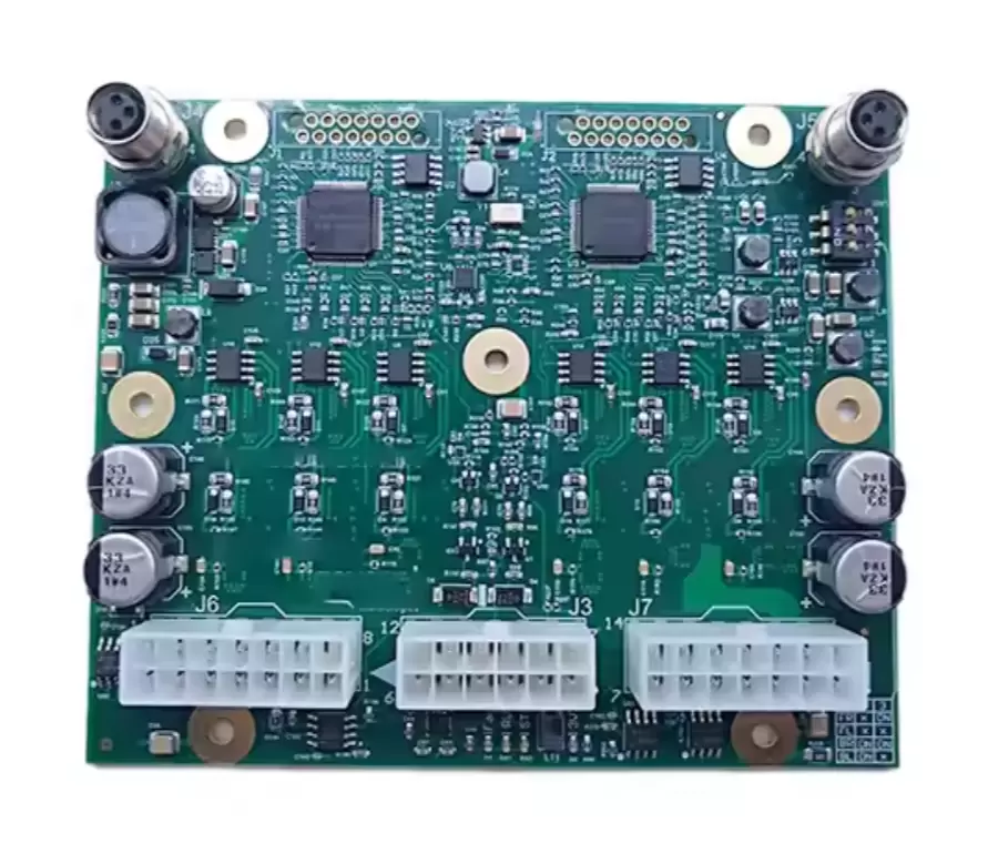
WiFi Wireless Smart Home IOT Module PCB Assembly
Case Study: WiFi Wireless Smart Home IoT Module PCB Assembly — Powering Connected Living with Reliable Connectivity
In the era of smart homes, IoT modules serve as the invisible bridges linking devices to networks, enabling seamless control of everything from smart lights to thermostats. A leading smart home technology provider partnered with us to address key challenges in assembling PCBs for their WiFi-enabled IoT modules, focusing on stable wireless performance, miniaturization, and low-power efficiency.
Project Background & Client Requirements
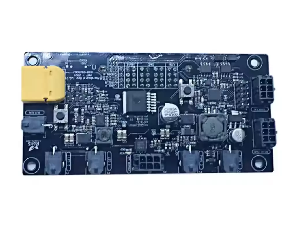
The client’s IoT module is a compact, multi-functional device designed to integrate with various smart home appliances (e.g., security cameras, smart locks, environmental sensors). Its PCB needed to:
· Support dual-band WiFi (2.4GHz/5GHz) with stable connectivity (≤1% packet loss at 50m range) and low latency (<50ms).
· Fit within a 35mm×25mm form factor to enable integration into space-constrained appliances.
· Operate on 3.3V DC with ultra-low standby power (<100μA) to extend battery life in wireless devices.
· Meet global IoT standards (CE, FCC, RoHS) for radio frequency (RF) emissions and safety.
· Scale from prototype (200 units) to mass production (20,000 units/month) with consistent performance.
Key Challenges in WiFi Smart Home IoT Module PCB Assembly
The project posed unique hurdles tied to the module’s wireless functionality and compact design:
1. RF Signal Integrity: WiFi signals (especially 5GHz) are highly sensitive to PCB layout, component placement, and solder joint quality—even minor inconsistencies can cause signal loss or interference.
2. Miniaturization Complexity: Packing a WiFi chipset, antenna, power management IC, and 01005 passives into a 35mm×25mm PCB increased the risk of component crowding and solder bridging.
3. Power Efficiency: Any inefficiency in PCB traces or component soldering could raise standby power consumption, undermining the module’s low-power design.
4. Regulatory Compliance: Strict RF emission limits (e.g., FCC Part 15) required precise control over antenna placement and grounding to avoid non-compliance.
Our Tailored Assembly Solutions
To overcome these challenges, we developed a “RF-optimized + precision-driven” strategy combining design collaboration, advanced assembly techniques, and targeted testing:
1. PCB Design & RF Optimization
· Layout Engineering: Collaborated with the client’s design team to optimize the PCB layout for RF performance:
· Separated RF circuits (WiFi chip, antenna) from digital/analog components (MCU, sensors) with grounded isolation walls to reduce noise.
· Designed a 50Ω microstrip line for the antenna feed, with controlled trace width (0.25mm) and spacing from ground planes to ensure impedance matching.
· Material Selection: Used high-frequency FR-4 substrate (DK=4.2) with low loss tangent (0.002) to minimize RF signal attenuation, paired with ENIG (Electroless Nickel Immersion Gold) surface finish for stable solder joint conductivity.
· Antenna Integration: Selected a chip antenna with PCB-mount design, placing it at the module’s edge to reduce interference from nearby components and ensure omnidirectional coverage.
2. Precision Assembly for Compact, High-Density Layouts
· Solder Paste Printing: Used a laser-cut stainless steel stencil (0.1mm thickness) with micro-apertures (0.15mm diameter) to apply precise solder paste volumes on 01005 component pads and the WiFi chip’s 0.4mm-pitch QFN pins. 3D SPI (Solder Paste Inspection) ensured paste volume accuracy (±8%) to prevent bridging.
· Component Placement: Deployed Yamaha YSM20R pick-and-place machines with high-resolution vision systems (0.5μm pixel size) to place tiny components (01005 resistors/capacitors) and the WiFi chip with positional accuracy of ±2μm—critical for maintaining RF trace integrity.
· Reflow Soldering: Customized a nitrogen-environment reflow profile to reduce oxidation, with peak temperature 250°C±1°C and slow cooling to minimize thermal stress on the WiFi chip, ensuring stable RF performance post-assembly.
3. Rigorous Testing & Compliance Validation
· RF Performance Testing:
· Conducted signal strength (RSSI) and throughput tests in an anechoic chamber, verifying 2.4GHz/5GHz connectivity with <0.5% packet loss at 50m.
· Measured antenna efficiency (>70% at 2.4GHz, >65% at 5GHz) and ensured compliance with FCC/CE RF emission limits (e.g., <30dBm EIRP for 2.4GHz).
· Electrical & Functional Testing:
· In-circuit testing (ICT) to verify component values and solder joint integrity, with special focus on power management ICs to ensure low standby current (<80μA).
· Functional validation via a custom test fixture: Simulated smart home commands (e.g., “turn on light”) to confirm response time (<30ms) and reliable data transmission.
· Environmental & Reliability Testing:
· Temperature cycling (-40°C to 85°C, 500 cycles) to test performance in extreme conditions, with RF signal strength monitored at each cycle.
· Vibration testing (10Hz-2000Hz, per IEC 60068-2-6) to simulate shipping and installation stress, ensuring no component detachment or signal degradation.
Project Outcomes & Client Impact
· RF Excellence: The module achieved stable dual-band WiFi connectivity with <0.3% packet loss at 50m and latency <25ms, exceeding the client’s performance targets.
· Regulatory Compliance: Passed FCC Part 15 and CE RED certifications on the first attempt, enabling global market entry without delays.
· Production Scalability: Scaled from 200 prototypes to 20,000 units/month with 99.3% yield, supported by automated testing that reduced inspection time by 50%.
· Power Efficiency: Standby power consumption measured at 75μA, extending battery life in wireless devices by 20% compared to the client’s previous module.
Why Choose Us for Smart Home IoT Module Assembly?
WiFi-enabled smart home IoT modules demand expertise in RF performance, miniaturized assembly, and regulatory compliance—areas where our 14-year focus on high-precision PCB assembly shines. We understand that reliable connectivity is the backbone of smart living, and our processes are designed to deliver modules that keep devices connected, efficient, and ready for global markets.