 en
en
PCB Facility
Advanced Equipment, Building High-Reliability PCBs
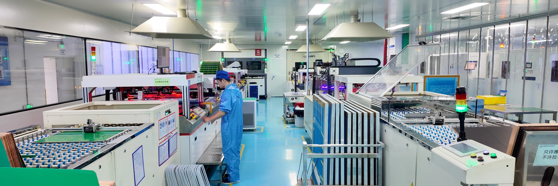
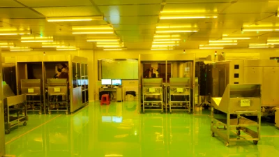
Step into Shenzhen Benlida, a professional PCB manufacturer with a modern PCB manufacturing facility designed for precision, efficiency, and scalability.
As an experienced PCB factory in China, we specialize in PCB fabrication and custom PCB manufacturing for global industries. Our production environment combines advanced automation with strict process control to ensure every printed circuit board meets high-performance standards.
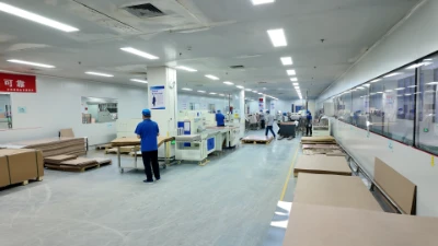
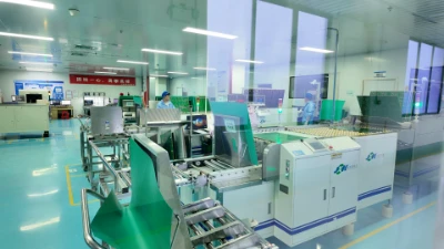
Our facility supports full-cycle PCB manufacturing, covering every stage from raw material preparation to final delivery:
1. Preparation and precision cutting
2. Inner layer imaging and etching
3. AOI inspection after etching
4. Multilayer lamination process
5. Drilling and hole formation
6. Image transfer and circuit development
7. Etching and pattern formation
8. Solder mask application
9. Silkscreen (legend printing)
10. Electrical testing (flying probe & fixtures)
11. Final inspection and packaging
This integrated workflow ensures consistent quality across multi-layer, HDI, flexible, and rigid PCB production.
 Preparation and Cutting | 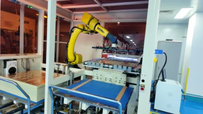 Inner Layer Etching | 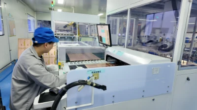 AOI after Etching | 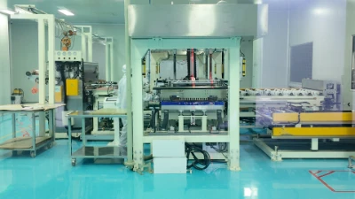 Lamination |
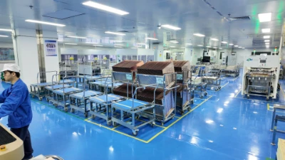 Brown Oxidation | 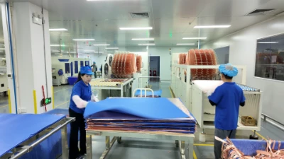 Prepare for Multi-layer Lamination | 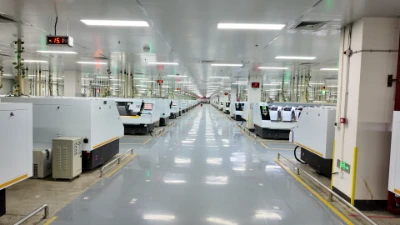 Drilling & Drill Shop | 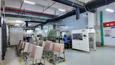 Image Transfer |
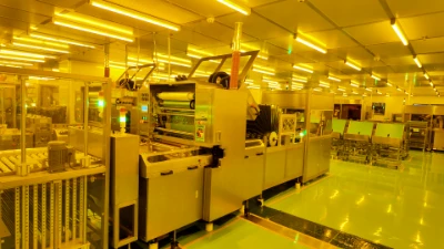 Image Transfer | 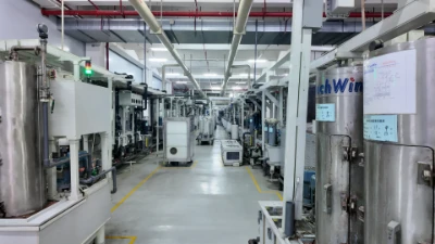 Etching Equipment | 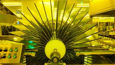 Etching Process | 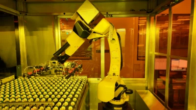 Etching Process |
 Etching Process | 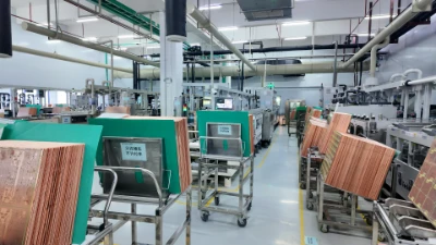 Etching Process | 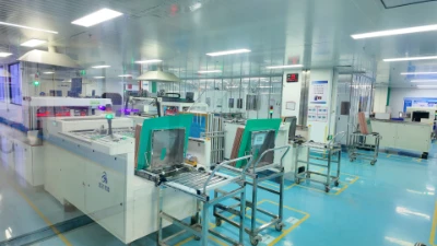 Solder Mask | 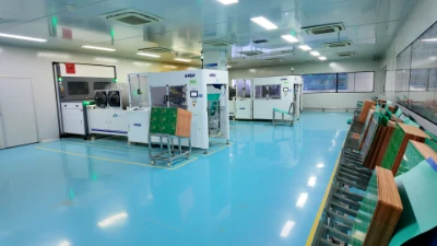 Solder Mask |
 Solder Mask | 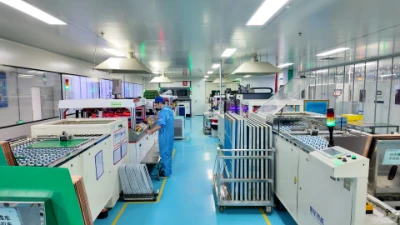 Legend / Silkscreen | 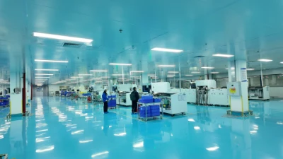 Electrical Test (Flying Probe & Fixture) | 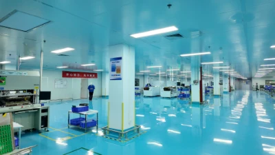 Electrical Test (Flying Probe & Fixture) |
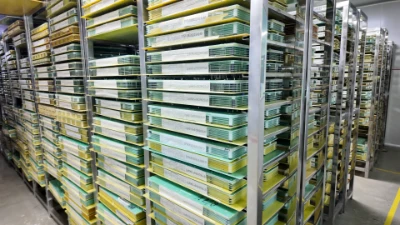 Testing Fixture Storage | 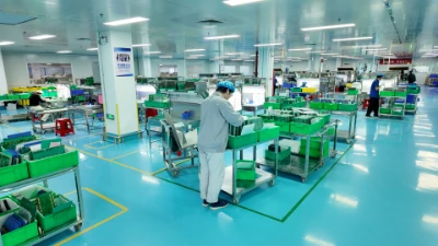 Appearance Inspection | 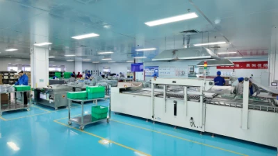 Packaging | 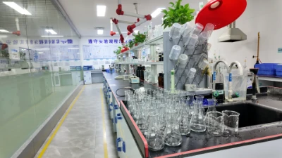 Chemical & Physical Lab |
| Item | Capability |
|---|---|
| PCB Types | Rigid PCB, Flexible PCB, Rigid-Flex PCB, HDI PCB |
| Layer Count | 1–20 Layers |
| Min Line Width/Spacing | 3/3 mil |
| Min Hole Size | 0.2 mm |
| Surface Finishes | HASL, ENIG, OSP |
| Board Thickness | 0.4–3.2 mm |
| Max Panel Size | 600 x 1200 mm |
| Production Volume | Prototype to mass production |
Quality is at the core of our PCB manufacturing process. Our factory is equipped with:
1. Automated Optical Inspection (AOI)
2. Electrical testing (flying probe & test fixtures)
3. Appearance inspection systems
4. Testing fixture management
5. In-house process monitoring
With advanced equipment, experienced engineers, and strong PCB manufacturing capability, Shenzhen Benlida delivers reliable PCB solutions worldwide.
Contact us today to get a fast quote for your custom PCB project.

 WhatsApp