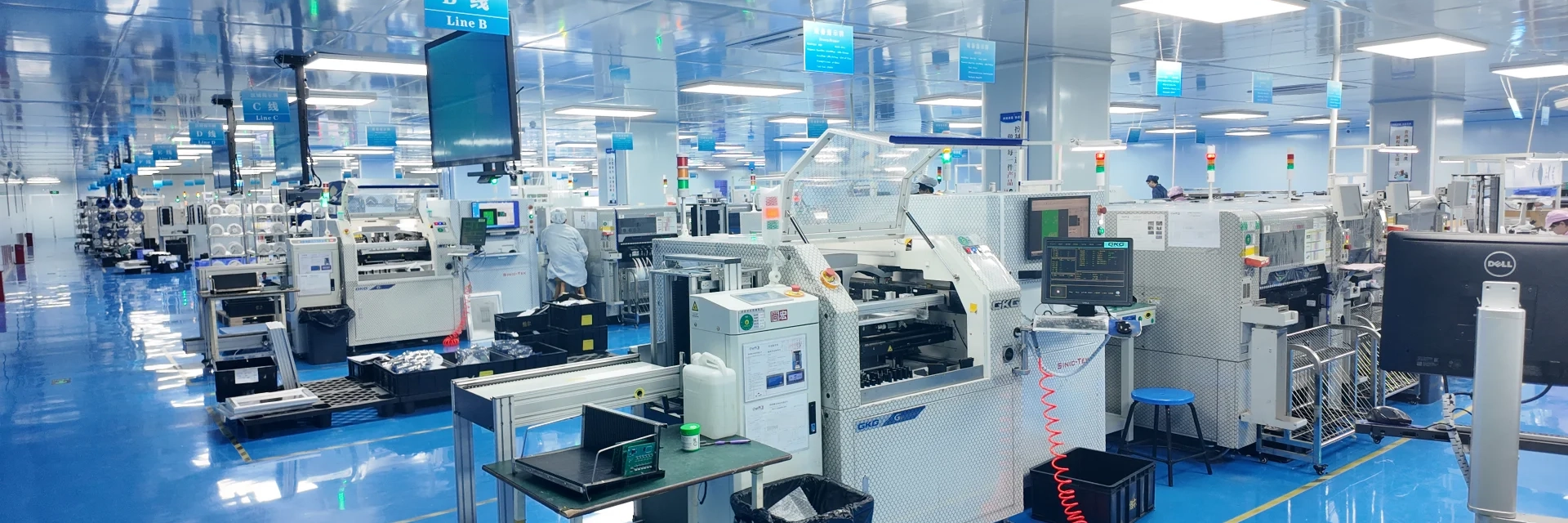
Our factories provide high -quality SMT assembly services for medical, aerospace, national defense industry, automobiles, communications and consumer electronics.
Surface Mount Technology (SMT) is a methodology for mounting electronic components directly onto the surface of a Printed Circuit Board (PCB). This process utilizes robotic systems to precisely position miniature components onto designated PCB pads. Assembly is finalized through reflow soldering or wave soldering techniques. SMT offers advanced automation and exceptional precision, significantly boosting manufacturing efficiency while minimizing human error, making it the dominant solution in contemporary electronics production.
Our facility boasts cutting-edge manufacturing infrastructure and sophisticated machinery to ensure superior fabrication. We employ highly skilled and seasoned specialists dedicated to delivering rapid turnaround times without compromising on quality. Our comprehensive capabilities in premium SMT PCB assembly services encompass:
X-ray
For PCBA (Printed Circuit Board Assembly) quality management, X-ray inspection is a key non-destructive inspection technology, primarily to inspect defects which hidden or covered by packages, such as solder balls of BGA, that cannot be checked by visual inspection(bare-eye) and electrical testing.
此处在右侧放置视频,方便读者点击观看
I. Principles of X-ray Inspection
Different materials have different absorption rates of X-rays (e.g., metals have high absorption rates, plastics/silicon have low absorption rates), thus X-ray could penerate the subjects and forming high-contrast, two-dimensional or three-dimensional images on the dispaly such as computor screen, thus revealing the internal structure.
II. Main Inspection Items
1. Soldering Quality Analysis
- Hidden solder joints such as BGA/CSP/QFN: Detecting solder ball voids, bridging/short, cold solder joints, misalignment, etc.
- Through-hole soldering: Checking for insufficient solder filler, porosity, and insertion deviation.
- Solder paste printing quality: Assessing the amount and uniformity of solder paste distribution (must be checked before reflow soldering).
2. Internal Structural Defects
- Interlayer Alignment: Misalignment of inner layers in multilayer PCBs.
- Wire/via integrity: Inspect for cracks, breaks, and uneven copper plating on via walls.
- Internal component defects: Such as chip package cracks, poor wire bonding, and voids.
3. Alien Objects and contamination
- Residual metal debris, fibers, and other conductive foreign objects.
4. Assembly verification
- Component misassembly, omissions, and reverse polarity (identified by shape and internal structure).
- Potential short circuit risk due to insufficient pin spacing.
III. Technical advantages
- Non-destructive imaging: Does not damage the PCBA, suitable for full inspection or sampling.
- High resolution: Micrometer-level identification (e.g., cracks <1μm).
- Automated analysis: With AI algorithms, automatically marks and classifies defects (e.g., void rate calculation).
- Fault Analysis: Root cause analysis of returned parts.
VII. Limitations
- High Cost: High investment and maintenance costs.
- Inspection Speed: 3D scanning is time-consuming, potentially affecting production cycle time.
- Material Limitations: High-density metal shielding layers (such as thick copper foil) may affect image quality.
- Radiation Safety: Strict management of operator protection and equipment shielding is required.
VIII. Technological Development Trends
- AI and Machine Learning: Automatic Defect Identification (ADI) systems reduce human error.
- Online Integration: Linked with SMT production lines to achieve real-time process feedback.
- High Resolution and High-Speed Scanning: Micro-focus X-ray and rapid CT improve inspection efficiency.
- Multimodal Data Fusion: Combining infrared thermal imaging, ultrasonic data, and other data for comprehensive judgment.
IX. Implementation Recommendations
1. Define Inspection Objects: Define inspection standards based on key product characteristics (e.g., BGA solder joints, automotive ECU modules).
2. Process Integration: X-ray data is fed back to the SMT process to optimize solder paste printing and reflow molding profiles.
3. Personnel Training: Operators must master basic image interpretation and equipment maintenance knowledge.
4. Data Management: A defect database is established for Statistical Process Control (SPC) and quality traceability.
X-ray inspection has become an important process of modern PCBA quality control, especially with the miniaturization and development of high-density electronic components, it's value is prominent. The proper application of this technology can improve product reliability and reduce after-sales risks significantly. Customers and manufacturers need to combine their own product characteristics and quality requirements, balance inspection costs and benefits, and formulate scientific inspection plans.
Benlida is a professional PCB and PCBA manufacturer, continuously invest in advanced equipment and had invested X-ray inspection equipment, provide customers with high-quality PCBs & PCBAs and excellent services continuously that keep up with the latest trends! If your PCBA requires X-ray inspection services, please contact Benlida!
This website uses cookies to provide you with a safer and more personal experience. By accepting, you agree to the Cookie Policy and the use of cookies for advertising and analytics purposes.
 en
en


 WhatsApp