 en
en

An Overview of PCBA Warpage: From Material to Manufacturing Process
On SMT assembly line, a warped PCBA might pass through the transporting rails but it might expose issues in future, such as solder joint cracking, chip stress damage and even complete system failure. Warpage, this deformation occurring at the millimeter scale, is a potential risk to yield and reliability in high-density electronic assembly.
I. The Essence of Warpage: Microscopic "Stress Conflict"
PCBA warpage is not simply "unevenness.", it's core issue is the inability to release internal stresses which generated during the thermal process due to mismatched coefficients of thermal expansion among different materials, such as the PCB substrate, copper layers, components, and solder. This stress conflict persists throughout the entire manufacturing process.
II. Five Root Causes: Where Does Warpage Come From?
1. "Natural Defects" in PCB Materials and Design
● Asymmetry from Board's Core: Asymmetry in the number of prepreg layers and copper foil thickness on multilayer boards, like uneven material distribution in a "sandwich," inevitably leads to an imbalance of internal stress after curing.
● Large Copper Surfaces and Mesh Design: The significant difference in thermal shrinkage between solid copper surfaces in the power/ground layers, and areas only with traces is a major cause of localized warping. Failure to use a mesh-like copper layer for large-area copper pours is a common design mistake.
● Tg Value of Material: Low Tg materials (such as ordinary FR-4) enter into highly elastic state when going through reflow soldering at peak temperatures, making them more susceptible to irreversible deformation from gravity and stress.
2. The "Additive Effect" from Component Layout and Weight Imbalance
● Concentration of Heavy Components on One Side: Concentrating large BGAs, heatsinks, inductors, and connectors on one side of the PCB leads to significant deformation, due to their own weight and thermal stress at high temperatures.
● Asymmetrical Packaging: Excessive differences in the mass and volume of components on both sides of the board, exacerbate the imbalance of thermal strain.
3. "Thermal Shock" during SMT Processes
● Improper Reflow Soldering Profile: Excessively rapid heating/cooling rates result in excessive temperature differences along the PCB thickness, generating huge instantaneous thermal stress.
● Localized overheating during wave soldering: During selective soldering or wave soldering, fixture obstruction can cause uneven heating of the PCB's upper and lower surfaces, resulting in arched warping.
4. "Chronic Erosion" from Environment and Stress
● Moisture Absorption and Deformation: PCBs (especially those using highly absorbent substrates) expand due to moisture absorption if being stored in humid environments. During reflow soldering, the rapid evaporation of moisture will lead to a "popcorn" effect and deformation.
● Residual Mechanical Stress: Mechanical stress accumulated during depaneling and assembly, if not fully released, will accumulate and manifest during the thermal process.
III. Improvement Methods
1. Design Optimization: Mandate symmetrical PCB layering, use a grid pattern for large copper areas, and incorporate balancing copper blocks in the panel design.
2. Material Selection: For high-reliability electronic products, use medium-to-high Tg substrates, low CTE materials (such as modified epoxy resin, polyimide), or a "sandwich" structure to stabilize the core board.
3. Thermal Process Control: Optimize reflow soldering profiles, using a gentle curve of heating-holding-reflow, to minimize the surface temperature differences on PCB.
4. Progress Monitoring: Introduce automatic warpage measurement at key workstations (such as after reflow soldering), providing real-time data feedback for statistical process control.
5. Environment and Stress: Strictly control the storage humidity of PCBs and semi-finished products, and perform standard baking on moisture-absorbing materials before SMT.
6. Failure Analysis and Closed-Loop Analysis: Perform stress, thermomechanical simulation, and cross-sectional analysis on PCBs with excessive warpage to pinpoint the root cause and continuously improve the process.
IV. Measurement Standards and Acceptance Criteria
The PCB industry generally follows IPC-A-610 and J-STD-003 standards:
1. For PCB assembly with bottom-mounted devices such as BGAs: The maximum permissible warpage is typically 0.75% (i.e., for a board length of 300mm, the maximum bow height is 2.25mm).
2. Devices without bottom terminals: Maximum permissible warpage can be relaxed to 1.0%-1.5%.
3. Measurement timing: Measurement must be taken at room temperature after the thermal process and before critical assembly.
Conclusion:
PCBA warpage is the result of multiple factors. To avoid warpage, a product-centric approach is required: Design engineers, PCB manufacturers, SMT process engineers, and material suppliers must strictly control their processes. From PCB layout in the design process to temperature rise control in the reflow oven, a systematic understanding and precise control are required, to ensure the PCBA is capable to support a reliable electronic products.
Benlida has been manufacturing PCBs for 14 years. We own professional equipment and technicians to perform precise warpage measurements, supporting engineers to understand&analyze the underlying physical mechanisms and improve processes. We have a mature engineering team and laboratory equipment:
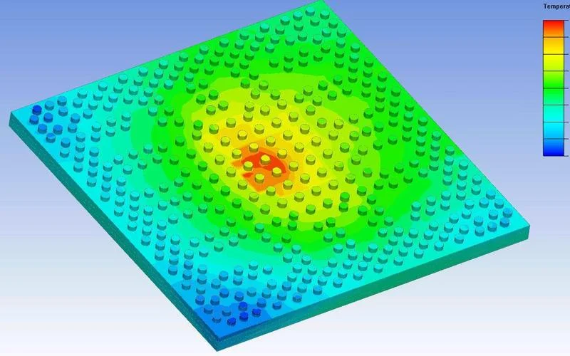
1. Precision 3D Warpage Measurement: Using a high-precision laser scanner and white light interferometer, generate 3D deformation cloud map of the entire PCBA surface.
2. Materials and Structure Analysis: analyze Tg and CTE of the substrate by using TMA and DSC. SEM/section analysis to observe the lamination structure, resin filling, and crack origin.
3. Thermal Stress Simulation and Verification: Thermomechanical finite element simulation is performed based on measured data to predict warpage risk and optimize process parameters.
4. Comprehensive Failure Analysis: A complete analysis report, from symptom to root cause, is provided for failures caused by warpage, such as open circuits, cold solder joints, and chip cracking.
If your PCB has warpage issues and you wish to systematically improve the quality of your PCB&PCBA, you are welcome to contact Benlida!
DISCOVER MORE
-
No Data
 WhatsApp