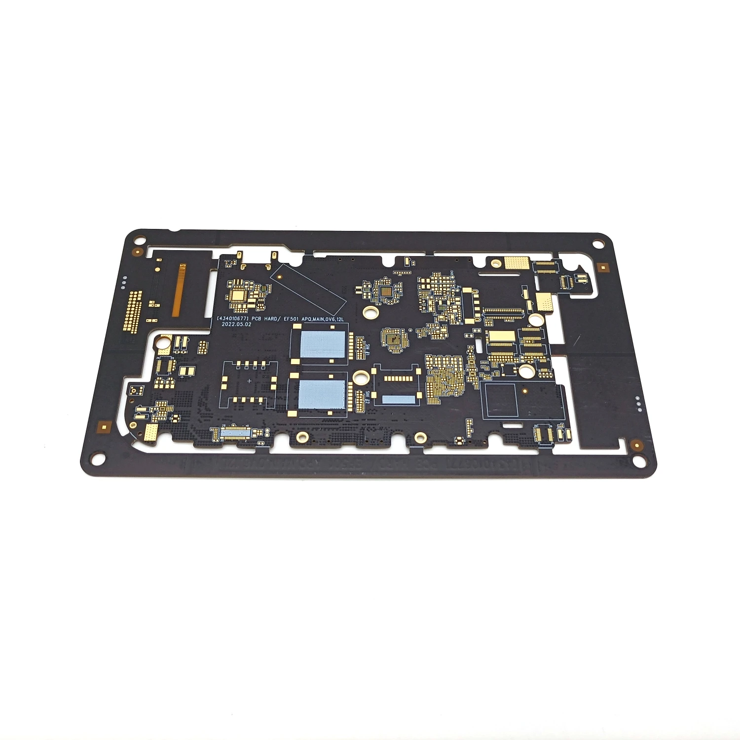
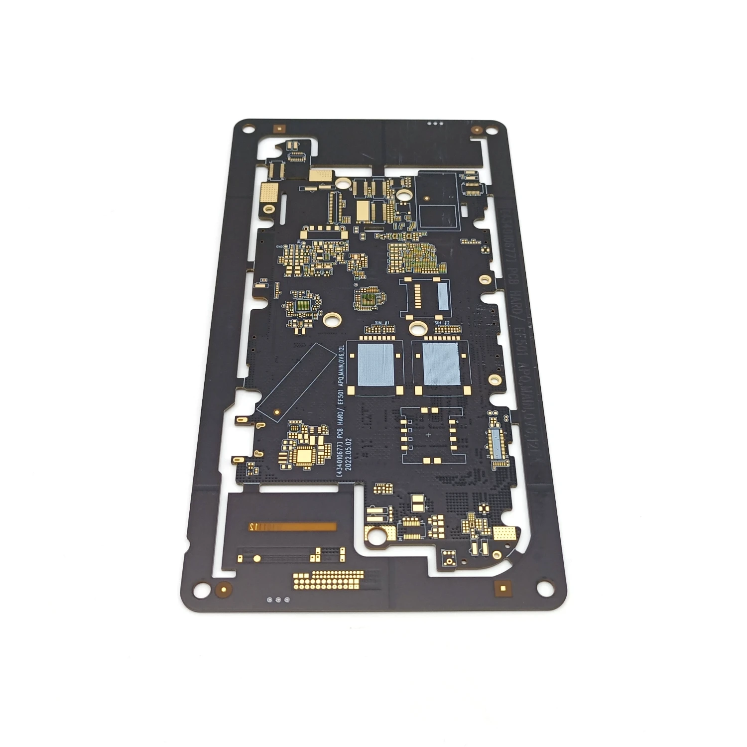
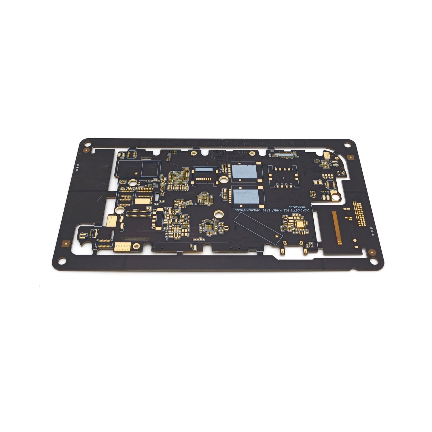
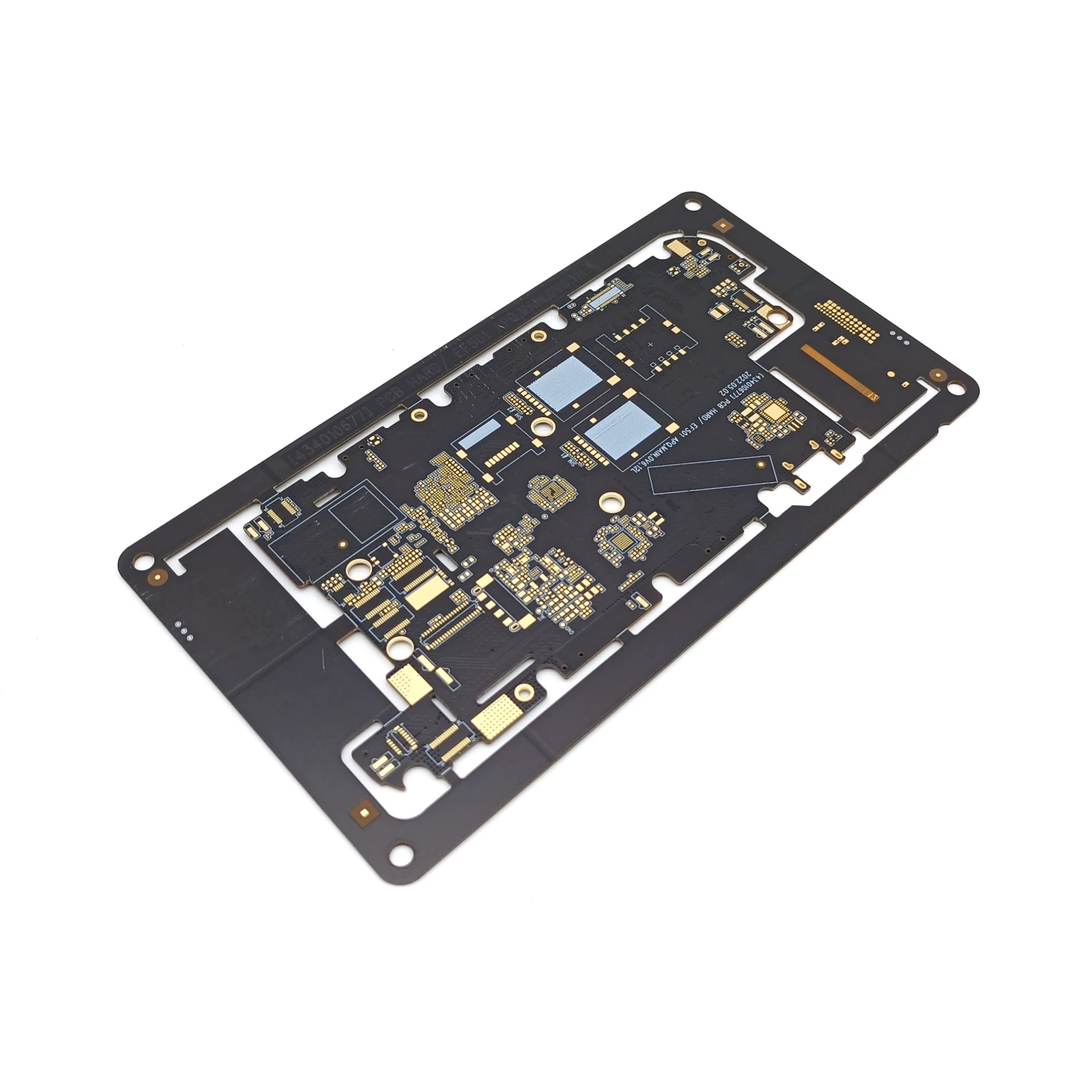
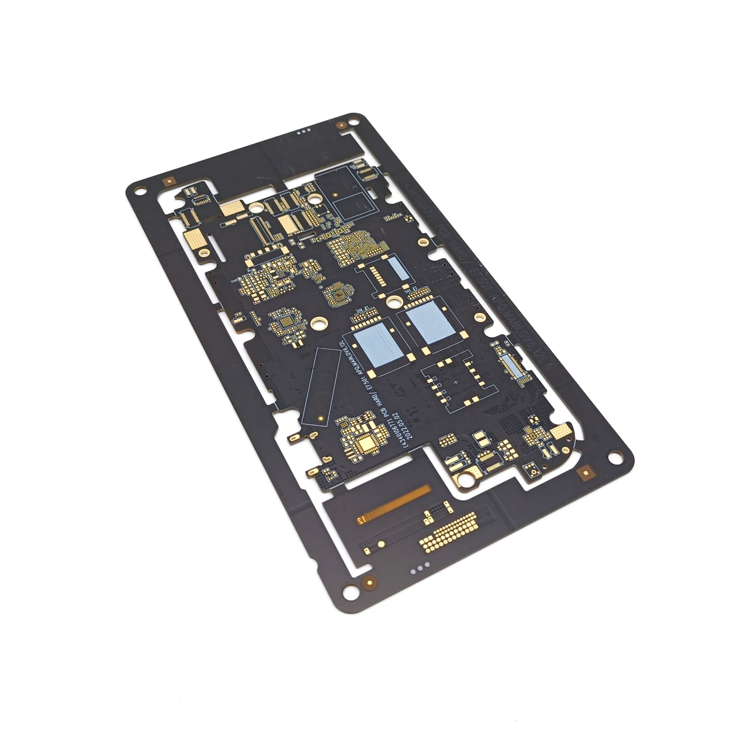
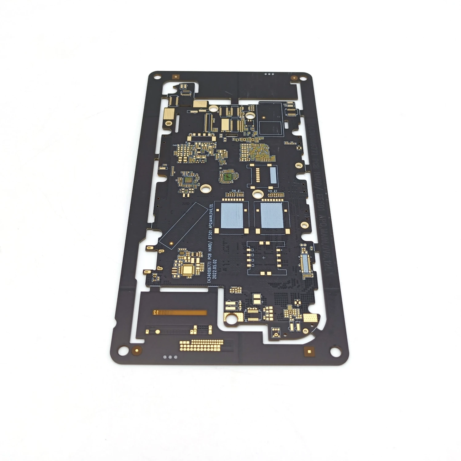
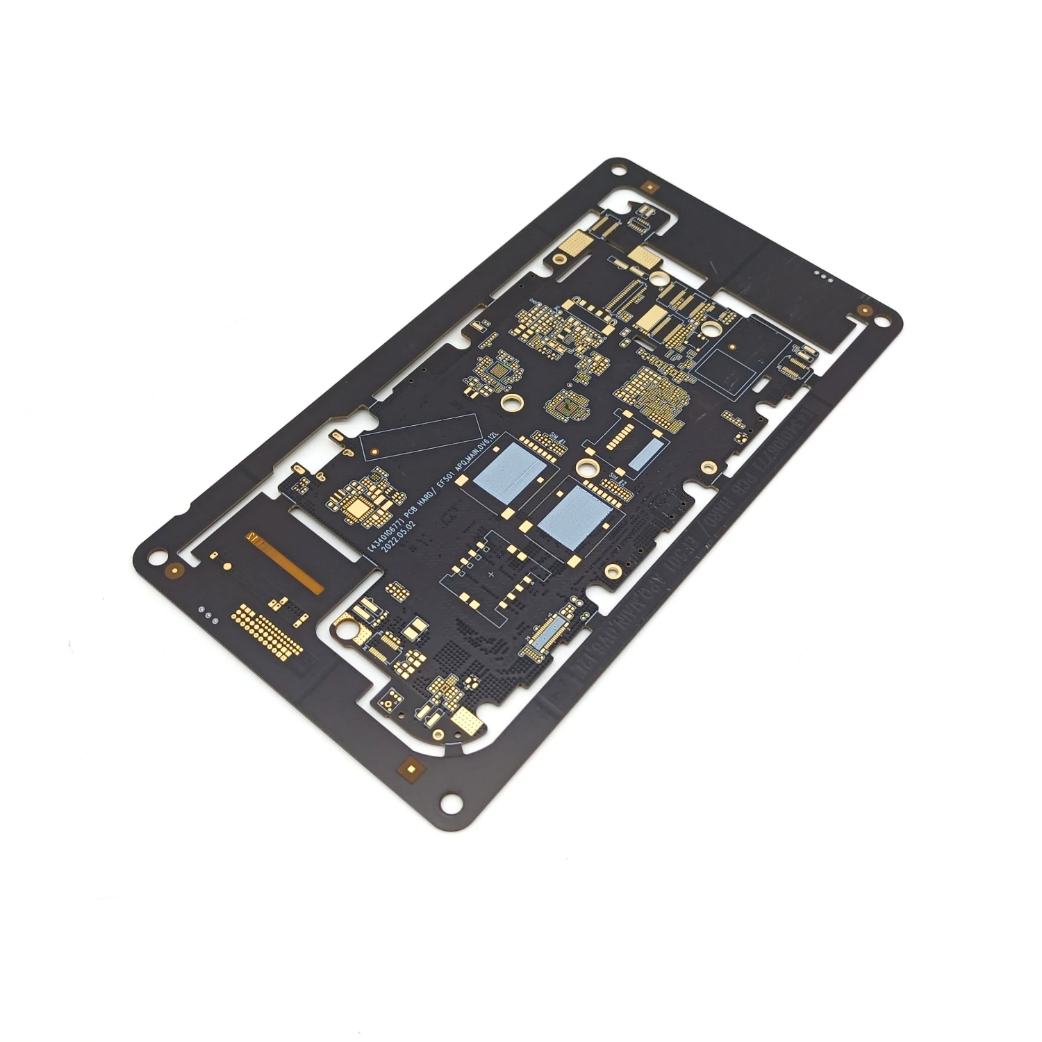
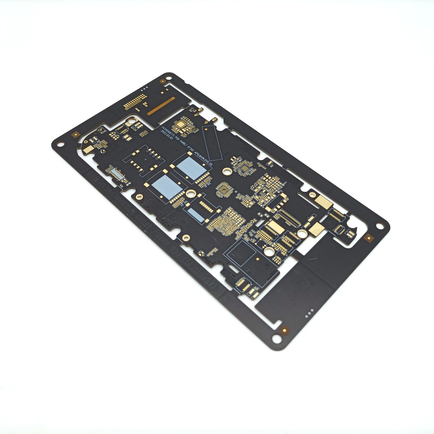
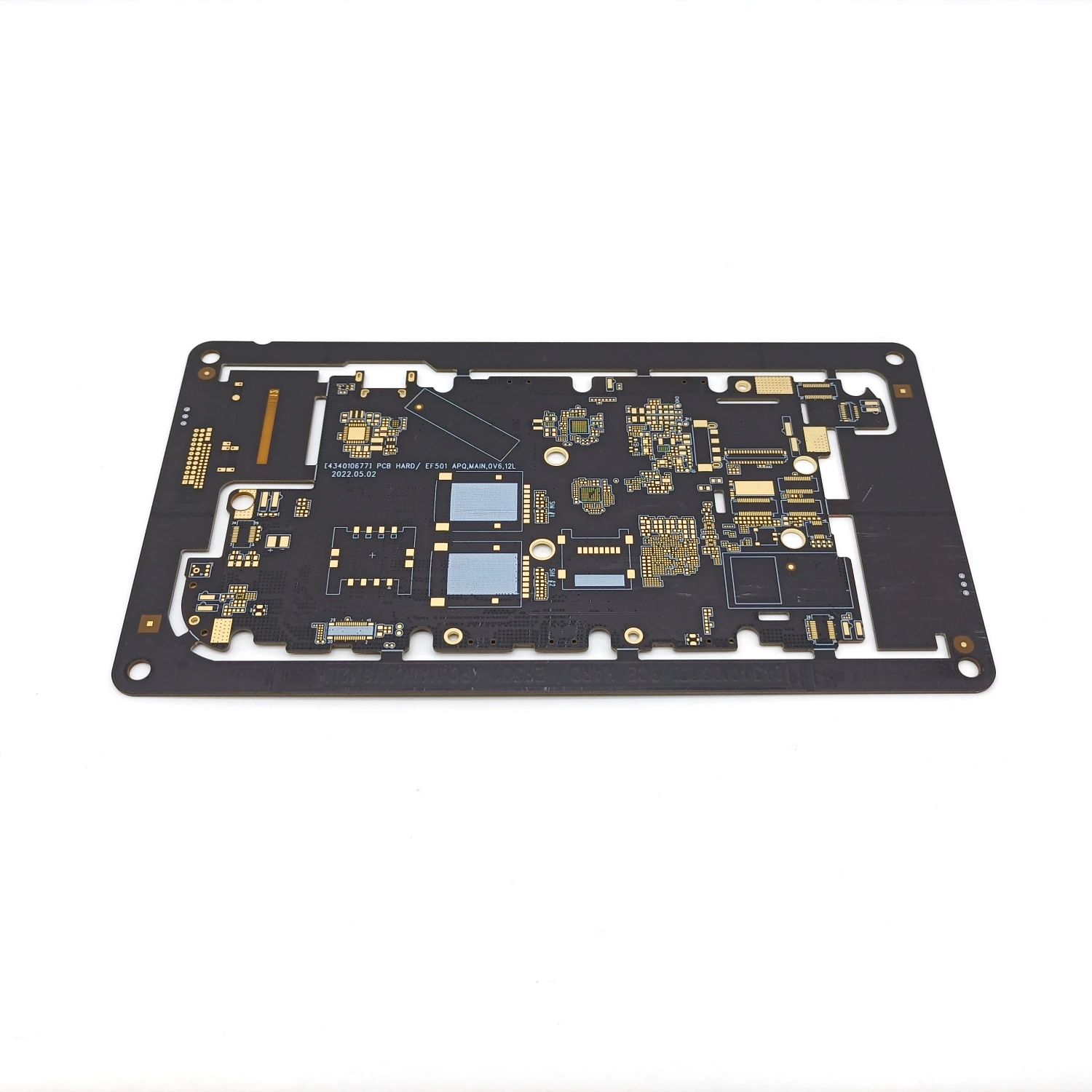
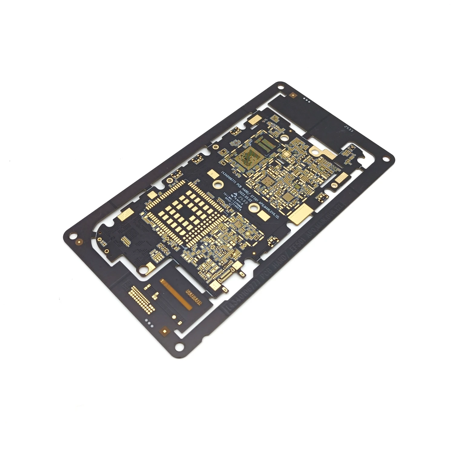
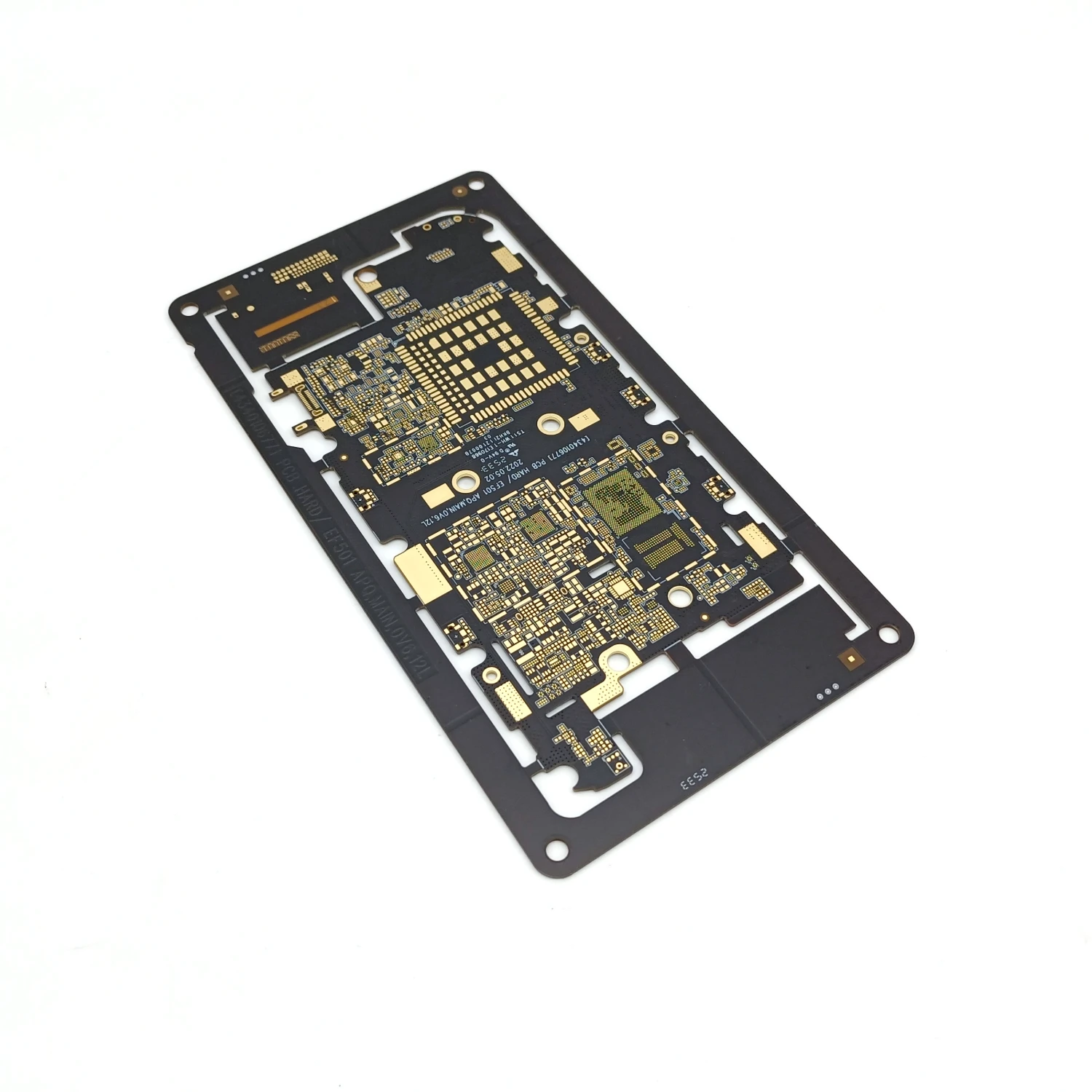
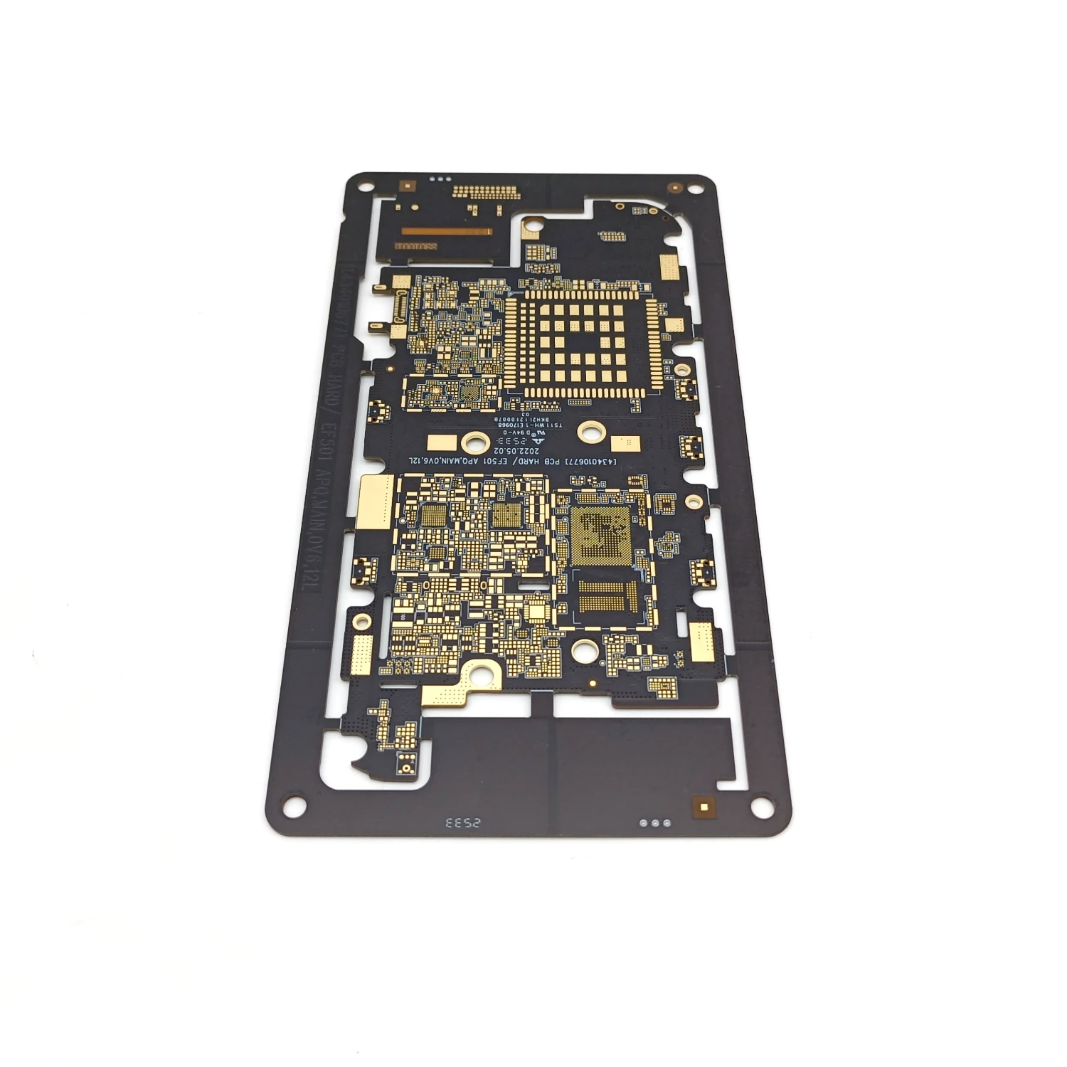
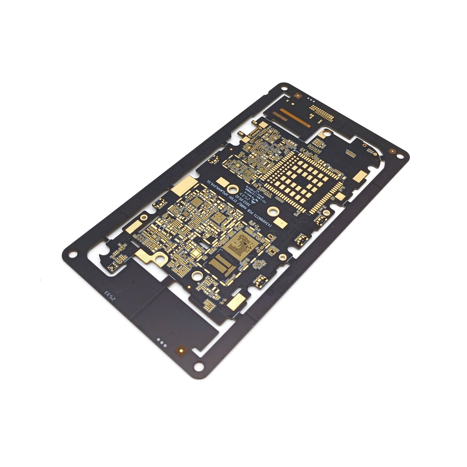
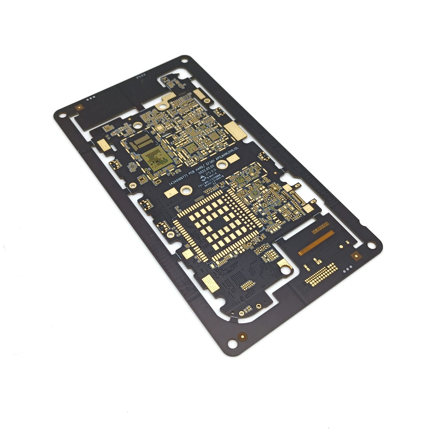
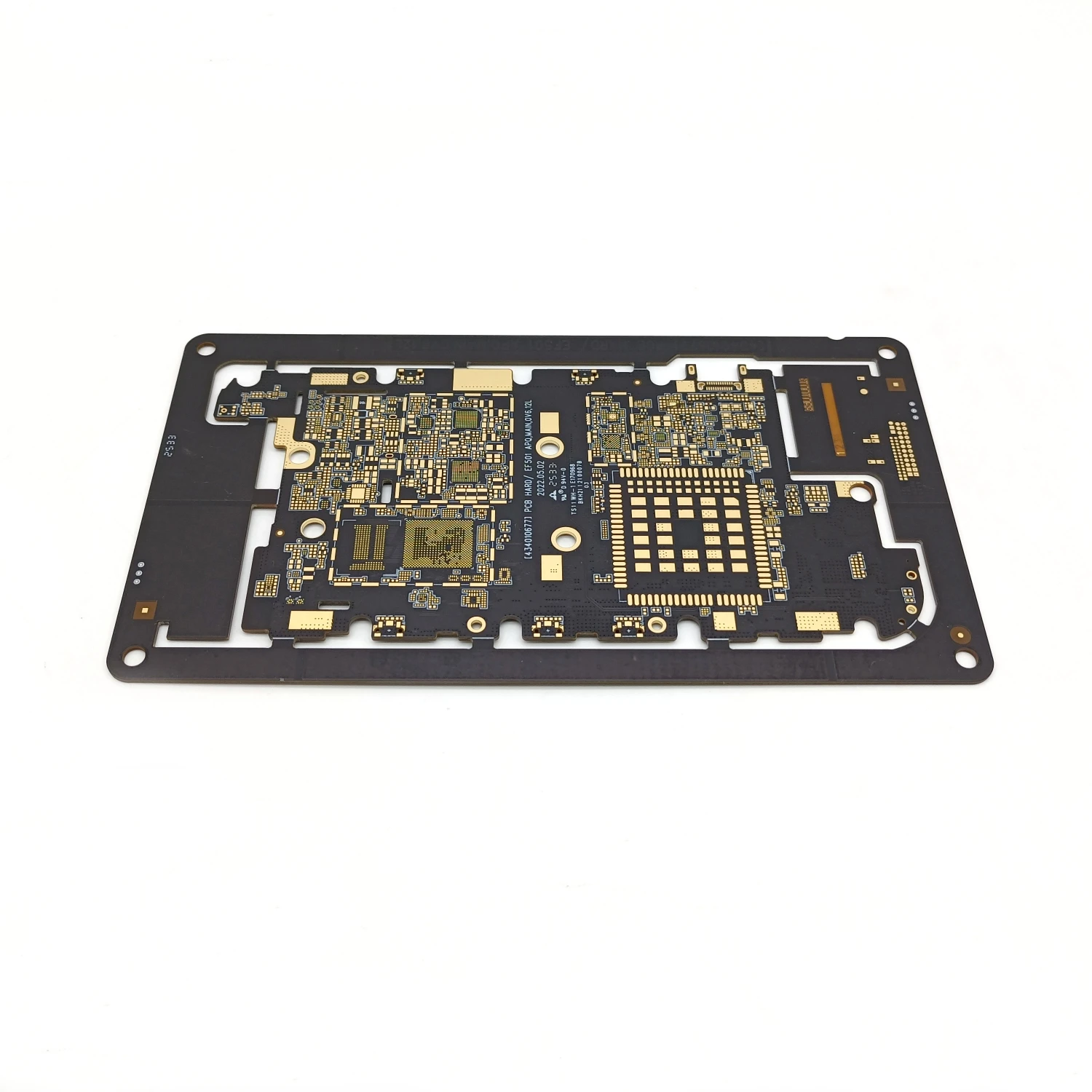
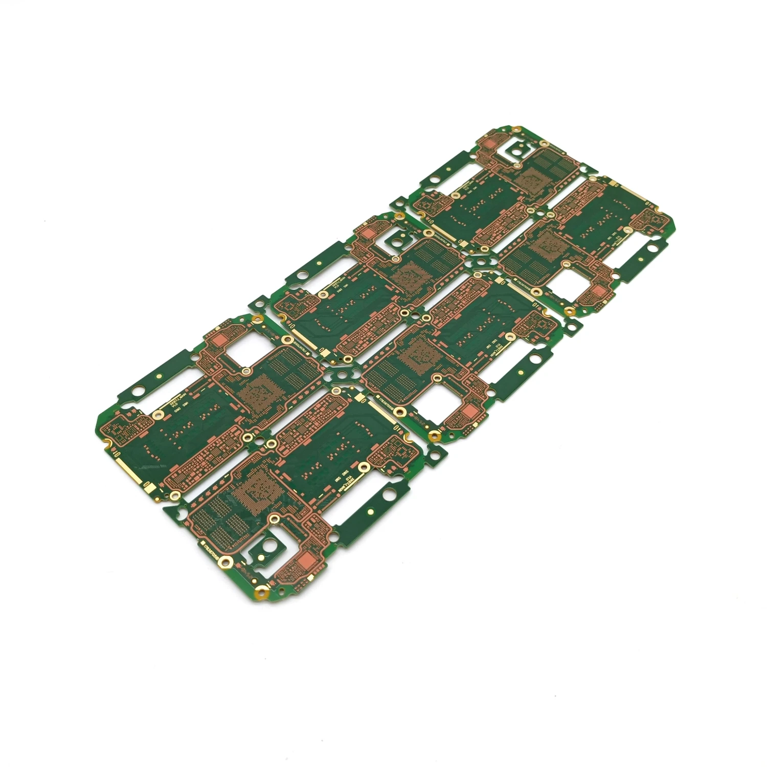
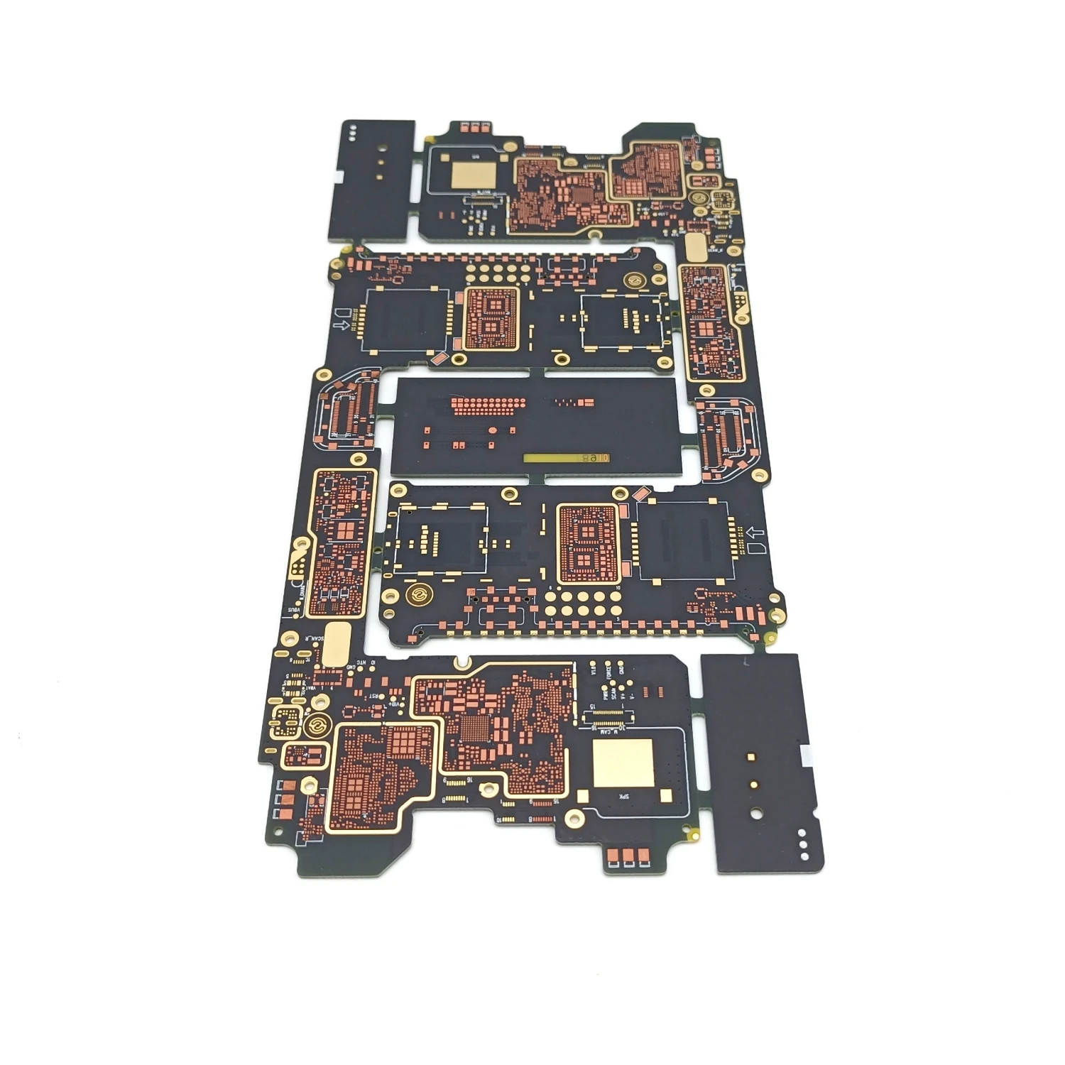
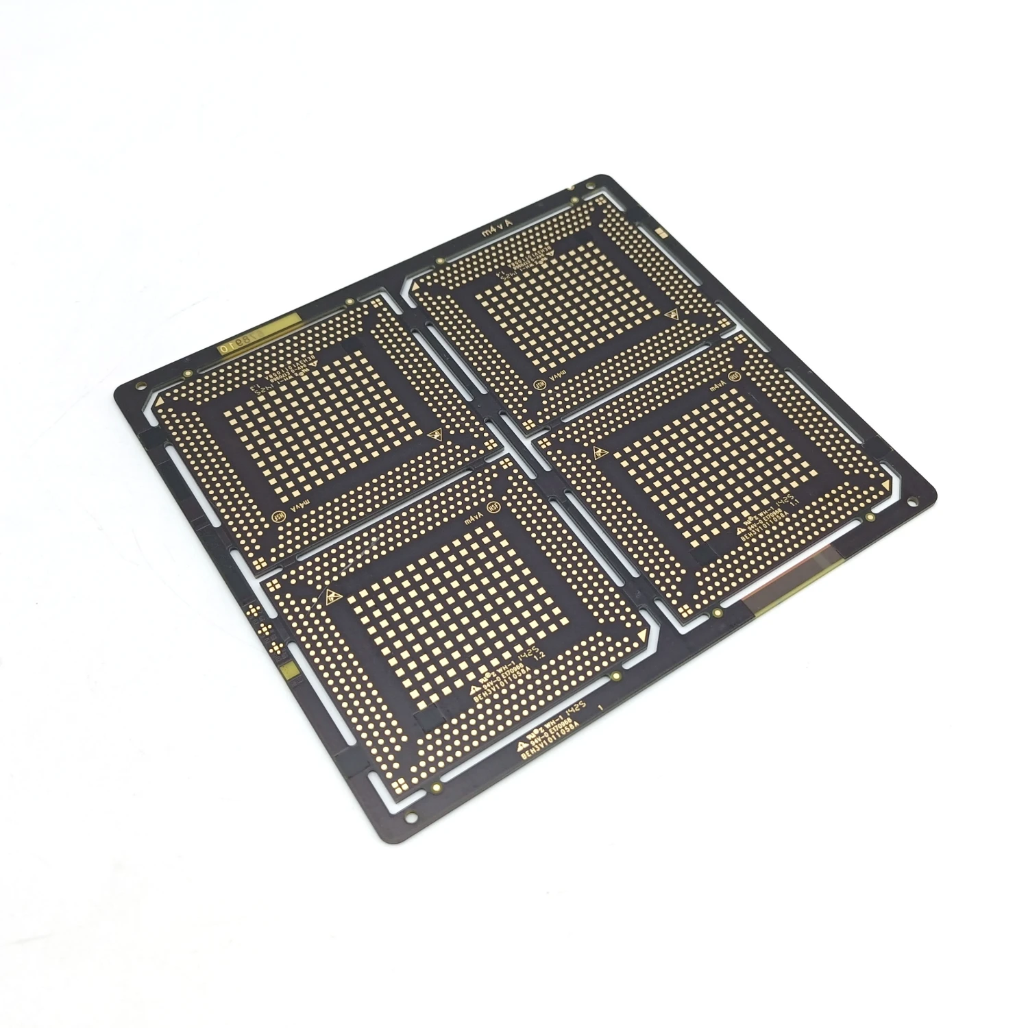
Home > PCB Fabrication Service > HDI PCB > HDI PCB Layers: 8 Sequence Type: 3+N+3

HDI PCB Layers: 8 Sequence Type: 3+N+3

HDI PCB (High-Density Interconnect Printed Circuit Board) is advanced circuit boards with much higher wiring density, smaller features (traces, vias, pads), and often more layers than traditional PCBs, achieved using technologies like microvias, blind/buried vias, and via-in-pad, leading to smaller, lighter, faster, and higher-performing electronics in demanding applications like smartphones, medical devices, and automotive systems. 

24-hour Quote

- Higher Density: More connections in the same area due to finer lines and spaces, allowing for more components and complex routing.

- Microvias: Very small holes (often laser-drilled) connecting layers, replacing larger, traditional drilled holes.

- Blind & Buried Vias: Vias that connect outer layers to inner layers (blind) or inner layers to other inner layers (buried), saving space.

- Via-in-Pad: Placing vias directly within component pads for direct connections, maximizing space.

- Improved Performance: Shorter signal paths, reduced reflections, better signal integrity, and faster speeds. 


Advantages of HDI PCBs
Miniaturization
Increased Functionality
Better Signal Quality

- Mobile Devices: Smartphones, tablets.

- Automotive: Advanced driver-assistance systems (ADAS), infotainment.

- Medical: Imaging, monitoring, surgical equipment.

- Industrial: Automation, IoT devices, smart sensors. 


Manufacturing Equipment at BENLIDA
contains the mostadvanced equipment required for the manufacture and assembly of your PCBs. Whether you'relooking for standard quick turn PCBs or boards with the tightest tolerances, made from exoticmetals, there's a reason Sierra Circuits leads the industry in quality and performance.
Tour the factory
24-hour Quote
  • Supported upload formats 锛歡tl锛実bl锛実ts锛実bs锛宐rd锛宻ch锛宬icad_pcb锛宬icad_sch锛実tl锛実bl锛実ts锛実bs锛宱db++锛2581锛宑sv锛寈ls锛寈lsx锛宑sv锛宼xt锛宲df锛宒wg