A PCB Anomaly Detection System Based on Computer Vision
Authors: Yang Yuxue, Lin Weiyang, Wang Bo, Li Huiming
Abstract
To address the challenges of high computational cost and poor adaptability in complex environments when detecting printed circuit board (PCB) defects on edge devices, a lightweight automatic detection system designed for edge deployment is proposed. The system is built upon the YOLOv8n architecture, integrating transfer learning, model pruning, and knowledge distillation techniques to significantly reduce model complexity and enhance adaptability to small-sample and resource-constrained environments. To handle extreme conditions in edge video acquisition such as variable lighting, conveyor vibration, low contrast, and lens occlusion, the system maintains both real-time performance and stability, demonstrating strong robustness. Experiments on a public PCB defect dataset show that the proposed system outperforms existing mainstream models in detection accuracy and inference speed, particularly exhibiting superior robustness and practical value in real-time edge detection scenarios. Additionally, a graphical user interface (GUI) developed using PySide6 further verifies the deployability and practicality of the system in industrial environments, providing an effective solution for achieving efficient, stable, and low-power edge vision detection with promising application prospects.
Keywords: Internet of Things (IoT); PCB defect detection; computer vision; YOLOv8; edge device; PySide6
0. Introduction
As an indispensable fundamental component of electronic products, the manufacturing quality of printed circuit boards (PCBs) directly affects the performance and operational reliability of the entire system. PCB defect detection aims to identify possible defects during the manufacturing process promptly and accurately, serving as a key quality control step in electronic production. However, in practical industrial environments, PCB defects exhibit complex characteristics—such as diverse types, small scales, and uncertain spatial distributions. Traditional detection methods based on manual inspection or rule-based logic are subjective and limited in capability, making them unable to meet the modern industrial requirements for high precision, efficiency, and automation.
With the rapid advancement of computer vision and deep learning technologies, convolutional neural networks (CNNs) designed for image recognition have achieved remarkable success in object detection tasks, promoting the transformation of PCB defect detection from manual feature extraction to intelligent feature learning. Nevertheless, mainstream deep learning models still face two major challenges in industrial deployment: (1) To achieve higher accuracy, models tend to become increasingly complex, leading to high computational costs and slow inference speeds, which hinders real-time detection on resource-limited edge devices; (2) Due to the scarcity of training samples specific to PCB defects, models trained on small datasets are prone to overfitting, thereby reducing generalization performance. Moreover, unlike general object detection tasks, PCB defect detection is characterized by fine-grained targets, weak semantic cues, and strong background noise interference, which imposes stricter requirements on the model’s robustness and deployment adaptability.
To address these challenges, this study designs and implements a lightweight and highly robust PCB defect detection system for edge computing environments. Specifically, the system is built upon the YOLOv8n framework, leveraging its compact structure and efficient inference capability to significantly reduce computational costs. During model training, transfer learning is adopted to migrate visual features pre-trained on large-scale general datasets to the PCB defect detection task, alleviating the difficulty of small-sample learning. Furthermore, model pruning and knowledge distillation are introduced to optimize the detection model’s architecture, compress its parameter scale, and improve deployment efficiency and stability on edge devices. To tackle challenges such as variable lighting, motion blur, and frame loss in industrial video acquisition, the system integrates a robust frame preprocessing and frame-level prediction stabilization module, enhancing reliability from a system-level perspective. Finally, a graphical user interface (GUI) based on PySide6 is developed to provide an intuitive and user-friendly experience, simplifying the operation workflow.
The research presented in this paper offers a practical solution for PCB defect detection on resource-constrained edge computing devices and provides new insights into model lightweighting and robustness optimization under small-sample conditions.
2. System Design and Implementation
2.1 Addressing Small Samples and Model Lightweighting
In PCB defect detection, data scarcity is a key factor limiting deep learning performance. Due to high annotation costs and limited defect data, achieving strong generalization with small samples has become a major research focus.
To mitigate this issue, transfer learning is employed to migrate features learned from large-scale source tasks to the target detection task, accelerating convergence and improving performance on small samples. Pre-trained YOLO models on general object datasets can serve as “teacher models” to guide “student models,” enhancing the detection of small defect targets.
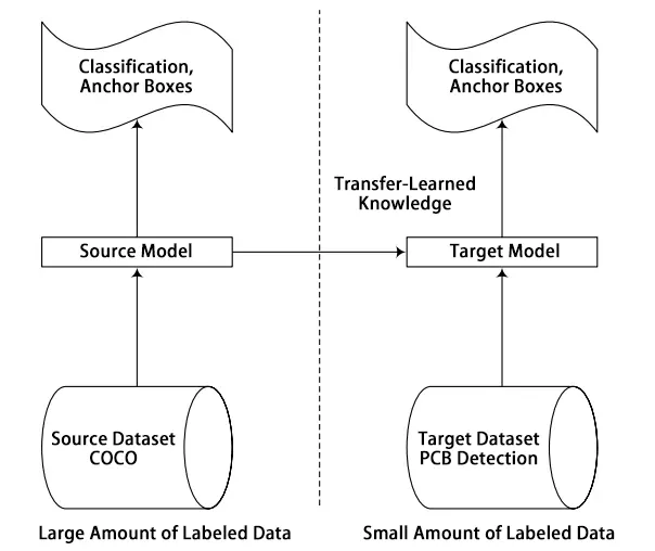
Figure 1. Principle of transfer learning
We adopt YOLOv8n—the lightest member of the YOLOv8 family [9]. With approximately 3.2×10⁶ parameters and 8.7×10⁹ FLOPs, it offers high-speed inference suitable for edge deployment. Further efficiency and adaptability are achieved via:
(1) Structural pruning: Prune redundant convolutional layers and channels in the YOLOv8n network to reduce parameters and computation.
(2) Knowledge distillation: Constrain the lightweight “student model” through guidance from a high-performance "teacher model," improving detection accuracy.
(3) Data augmentation: Adjust enhancement parameters in the HSV color space to increase sample diversity and model robustness.
As shown in Figure 2, the model training process includes data preparation, hyperparameter configuration, model training and evaluation, and pruning optimization. If the model's evaluation metrics do not meet expectations, parameters are automatically adjusted, and training and pruning are repeated until satisfactory detection performance is achieved.
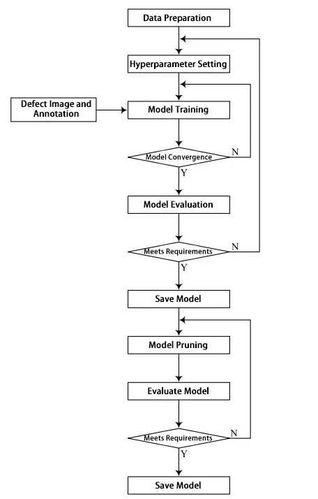
Figure 2 Model training process
2.2 Edge-Side System and Deployment
To meet the requirements for ease of use and deployment convenience in real industrial environments, an integrated PCB defect detection system was designed and implemented using the PySide6 framework. The system supports both image and video input modes, offering strong interactivity and a user-friendly experience suitable for deployment on edge devices. The system interface provides the following features:
(1) Support for multiple input sources, including single images, batch image folders, and video streams;
(2) Customizable detection parameters (confidence threshold, IoU threshold) and display options (show class labels, confidence levels, etc.);
(3) Real-time display and database storage of detection results;
(4) Extended functions such as detection record retrieval and bounding box information browsing.
The system's detection process includes user interface interaction, input source parsing, image/video detection thread management, and result updating. As shown in Figure 3, after the user selects the input type and sets parameters, the system automatically starts the corresponding image or video processing thread to perform frame-by-frame detection and display results.
Key system events include detection command events, target update events, detection list selection events, and background thread management events, as described in Table 1.
3. Experimental Results and Analysis
3.1 Dataset and Preprocessing
Experiments use the PKU-Market-PCB dataset released by Peking University [10]. It is synthetically generated with 1,386 high-resolution images and six defect types: Missing_hole, Mouse_bite, Open_circuit, Short, Spur, and Spurious_copper. Typical defects in the dataset are shown in Figure 4.
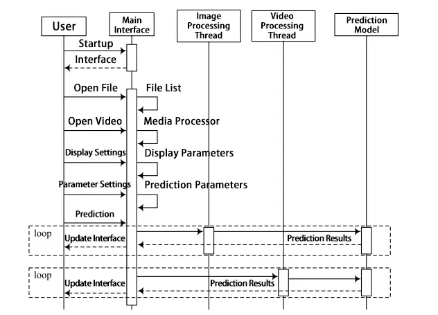
Figure 3 System detection timing
Table 1. Major Events of the System
| Event | Type | Description |
| Detection | Click | Start the image processing thread or media processing thread according to the detection type. |
| Media Processing Thread | — | Sequentially read images, perform detection, and update the result and bounding box list. |
| Image Processing Thread | — | Sequentially read images from the image list, perform detection, update and display the results and bounding box list, and remove processed images from the list. |
| Target Object | Change | Display the detection result of the selected bounding box. |
| List | Click | Display the detection result of the selected bounding box and show the corresponding detection image. |
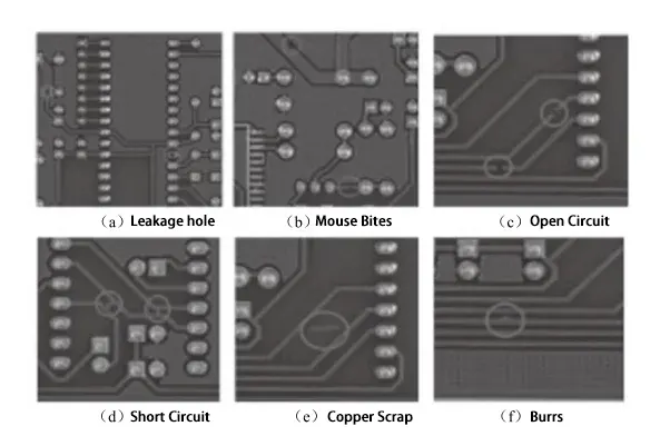
Figure 4 Typical defects on PCB surface
To ensure the scientific validity and robustness of model training, the entire dataset was divided into training, validation, and test sets in an 8:1:1 ratio. In the training set, defect targets are relatively small and distributed sparsely, increasing the difficulty of small-object perception and localization and imposing higher requirements on the detection system.
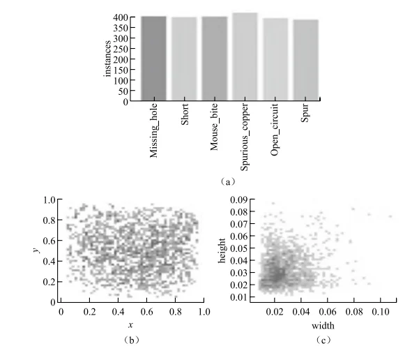
Figure 5. Training set data annotation information
3.2 Metrics
To comprehensively evaluate the performance of the defect detection model, the following evaluation metrics are used:
(1) Precision: Measures the proportion of true positives among all predicted positives, reflecting the model's resistance to false detections.
(2) Recall: Measures the model's ability to identify all true positive samples, reflecting resistance to missed detections.
(3) F1-score: The harmonic mean of Precision and Recall, reflecting the model's overall detection capability.
(4) mAP (mean Average Precision): The mean of average precision across all classes, used to evaluate the model's overall classification and localization performance.
The formulas for calculating Precision, Recall, F1-score, and mAP are as follows:
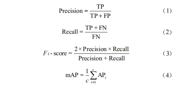
TP represents the number of correctly classified positive samples; FP represents the number of negative samples misclassified as positive; FN represents the number of positive samples misclassified as negative; c is the total number of image categories; i is the number of detections; and AP is the average accuracy of a single category.
3.3 System Implementation and Multi-Scenario Results
The detection system runs on an Ubuntu 23.04 platform equipped with an Intel Core i5-11400F (12 threads), 16 GB of memory, and an NVIDIA GeForce RTX 3060 GPU (12 GB VRAM). The inference deployment platform uses Windows 10 with an Intel i7-6600U processor and 8 GB of memory, while edge deployment is implemented on the NLE-AI800 edge computing development board produced by Beijing Newland Era Technology Co., Ltd. As shown in Figure 6, the detection system interface supports both image and video inputs, providing various configurable detection parameters and real-time result visualization.

Figure 6 Defect Detection System Interface
(1) Batch Image Detection Batch detection was conducted on a folder named "img2video" containing defect images. The detection results are shown in Figure 7. The folder includes 66 defect images, and by iterating through them one by one, a total of 269 defects were detected. Users can view each defect by clicking the corresponding item in the results list, which instantly highlights the defect in the image display window. Figure 8 demonstrates how clicking on the 235th detected defect (a missing hole) allows the system to quickly locate and display the corresponding image region.
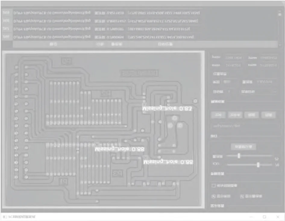
Figure 7. Batch Folder Detection Results
(2) Video Stream Detection The system supports frame-by-frame video detection mode. As shown in Figure 9, a video composed of 50 defect images was analyzed, and 282 defects were identified. The system also supports defect localization and frame backtracking, making it suitable for quality inspection scenarios in production line camera systems.
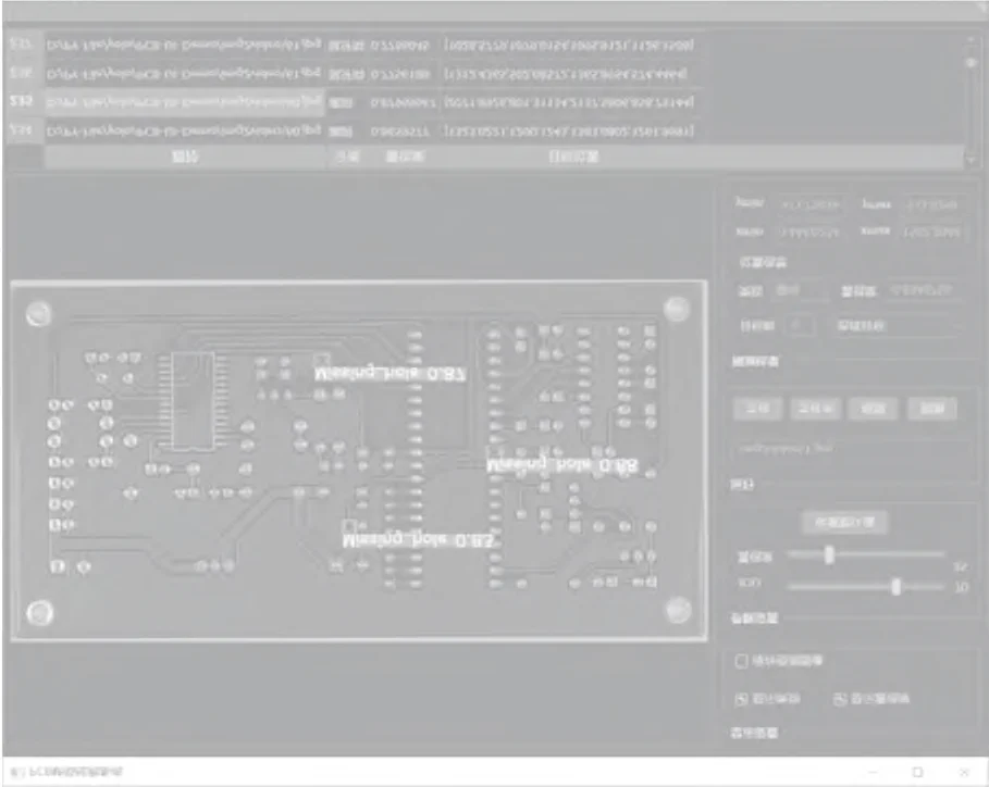
Figure 8. Detailed information on image defect detection results
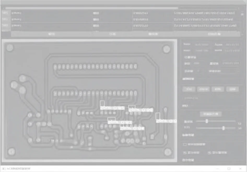
Figure 9. Video detection results
(3) Extreme Condition Detection To evaluate the system's robustness under extreme conditions, tests were conducted on images affected by "blurring," "occlusion," and "offset." As shown in Figure 10, the system successfully identified most defects even under these challenging conditions, indicating strong environmental adaptability.
(4) Edge Device Detection As shown in Figure 11, detection results from edge device deployment in real industrial settings demonstrate the system’s ability to identify typical defects such as short circuits, open circuits, and missing holes. The device achieves real-time performance while maintaining high accuracy, verifying the deployability of the proposed model in low-power scenarios.
3.4 Performance Evaluation
3.4.1 Evaluation of the Detection System's Model Training Results
The image size was set to 1,280×720 pixels, the batch size to 8, the number of training epochs to 300, and the initial learning rate to 0.01. As shown in Table 2, training concluded at the 206th epoch, and the optimal result was achieved at the 106th epoch. The inference time was 11.5 ms. The model achieved an average Precision of 0.98, an average Recall of 0.961, and an average mAP of 0.982 across all defect classes. Performance on Spurious_copper was slightly weaker, while Missing_hole and Short were predicted more accurately.
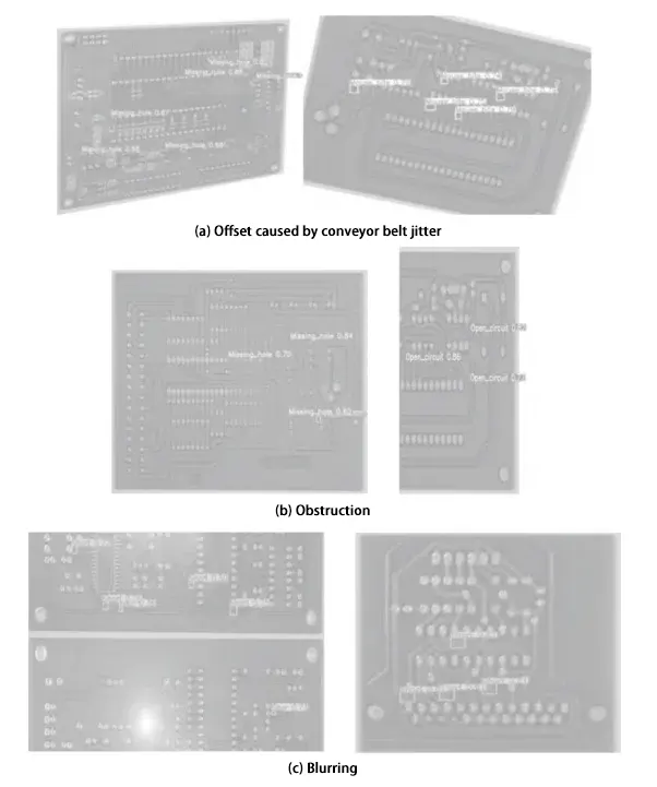
Figure 10. Detection results under extreme conditions
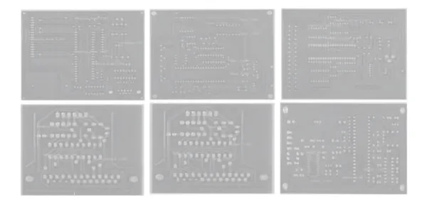
Figure 11. Edge detection results
3.4.2 Evaluation of the Detection System’s Model Prediction Results
Model prediction results are shown in Table 3 and are broadly consistent with the training-stage outcomes. Figure 12 compares correctly labeled defect images (rows 1 and 2) with predicted defect images (rows 3 and 4). The visualizations indicate strong overall performance, though a few missed detections (e.g., row 3, image 2) and false detections (e.g., row 4, image 3) are present.
3.4.3 Evaluation of the Detection System Performance
Precision and Recall are two key metrics for classification performance. Precision measures the proportion of true positives among predicted positives, while Recall measures the proportion of true positives correctly identified. Figure 13 shows how Precision, Recall, and F1-score vary with the confidence threshold. As seen in Figure 13(a), Precision increases with the threshold and reaches 1.0 across all classes at a threshold of 0.73; however, beyond this point Recall drops sharply. Based on the F1-score, a confidence threshold of 0.73 yields the best overall performance. The confusion matrix in Figure 14 visualizes predictions, showing strong overall performance but relatively weaker detection for classes with subtle inter-class differences (e.g., Spurious_copper and Spur).
Table 2 Model Training Results
| Defect Type | Total Images / pcs | Category Annotation Quantity | Precision | Recall | mAP@50 | mAP@50:95 |
| all | 66 | 280 | 0.980 | 0.961 | 0.982 | 0.563 |
| Missing_hole | 66 | 45 | 0.991 | 1.000 | 0.995 | 0.658 |
| Short | 66 | 45 | 0.999 | 1.000 | 0.995 | 0.562 |
| Mouse_bite | 66 | 49 | 1.000 | 0.938 | 0.992 | 0.593 |
| Spurious_copper | 66 | 43 | 0.940 | 0.953 | 0.985 | 0.477 |
| Open_circuit | 66 | 49 | 0.970 | 0.959 | 0.968 | 0.589 |
| Spur | 66 | 49 | 0.978 | 0.913 | 0.957 | 0.497 |
Table 3 Model Prediction Results
| Type | Total Images / pcs | Category Annotation Quantity | Precision | Recall | mAP@50 | mAP@50:95 |
| all | 66 | 280 | 0.967 | 0.968 | 0.982 | 0.565 |
| Missing_hole | 66 | 45 | 0.988 | 1.000 | 0.995 | 0.667 |
| Short | 66 | 45 | 0.993 | 1.000 | 0.995 | 0.563 |
| Mouse_bite | 66 | 49 | 0.979 | 0.939 | 0.992 | 0.586 |
| Spurious_copper | 66 | 43 | 0.917 | 0.953 | 0.986 | 0.479 |
| Open_circuit | 66 | 49 | 0.965 | 0.959 | 0.968 | 0.596 |
| Spur | 66 | 49 | 0.959 | 0.957 | 0.956 | 0.500 |
3.4.4 Comparative Experimental Evaluation of the Detection System
To further validate performance, the proposed model was compared against mainstream detectors on the public Peking University PCB defect dataset, with comparative data drawn from [11].As shown in Table 4, the proposed model achieves superior prediction accuracy and mean average precision (mAP) compared with the baselines.
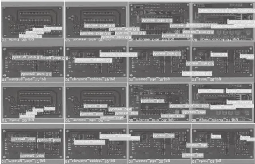
Figure 12. Comparison between correctly labeled defect images and predicted defect images
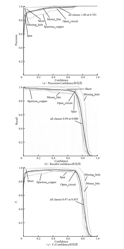
Figure 13 System performance evaluation results
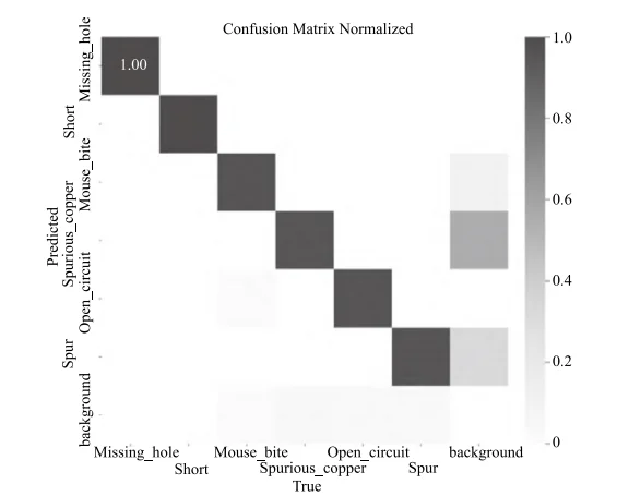
Figure 14. Visualization of evaluation results using the confusion matrix method
Table 4 Comparative Experimental Results (%)
| Model | Missing_hole | Mouse_bite | Open_circuit | Short | Spur | Spurious_copper | mAP |
| Faster R-CNN | 91.7 | 78.2 | 80.6 | 84.8 | 74.8 | 85.1 | 82.5 |
| YOLOx | 99.5 | 91.2 | 92.5 | 90.1 | 86.3 | 94.4 | 92.3 |
| PCB-YOLO | 99.5 | 90.7 | 99.5 | 98.5 | 90.9 | 96.7 | 95.9 |
| FCM-YOLO | 99.5 | 98.1 | 98.9 | 97.8 | 97.4 | 98.5 | 98.3 |
| Proposed Model | 98.8 | 97.9 | 96.5 | 99.3 | 95.9 | 91.7 | 96.2 |
4. Conclusion
To address the dual demands of real-time performance and resource constraints in edge computing scenarios, this paper designed and implemented a lightweight PCB defect detection system based on YOLOv8n. By integrating transfer learning, model pruning, and knowledge distillation techniques, the system significantly reduces model complexity and enhances detection performance in small-sample and complex environments. The graphical user interface (GUI) developed with PySide6 enables multi-modal input and interaction for both images and videos, offering excellent engineering adaptability and deployment flexibility.
Experiments conducted on a public dataset demonstrate that the proposed model outperforms existing mainstream methods in detection accuracy, inference speed, and robustness. It maintains stability even under challenging conditions such as occlusion, blurring, and device vibration. Deployment experiments on real edge devices further confirm the system’s feasibility under low-power and low-latency conditions, highlighting its strong potential for practical application and future deployment.
References
- [1] REN S., HE K., GIRSHICK R., et al. Faster R-CNN: Towards real-time object detection with region proposal networks. IEEE Transactions on Pattern Analysis and Machine Intelligence, 2017, 39(6): 1137–1149. ↩︎ Back to: [1]
- [2] HU K., WANG B., SHEN Y., et al. Defect identification method for poplar veneer based on progressive growing generative adversarial network and MASK R-CNN model. BioResources, 2020, 15(2): 3041–3052. ↩︎ Back to: [2]
- [3] REDMON J., DIVVALA S., GIRSHICK R., et al. You Only Look Once: Unified, real-time object detection. In Proceedings of the IEEE Conference on Computer Vision and Pattern Recognition, 2016: 779–788. ↩︎ Back to: [3]
- [4] LIU W., ANGUELOV D., ERHAN D., et al. SSD: Single shot multibox detector. In European Conference on Computer Vision. Springer, 2016: 21–37. ↩︎ Back to: [4]
- [5] Hu Xin, Hu Shuai, Ma Lijun, et al. PCB defect detection method based on the fusion of MBAM and YOLOv5. Journal of Graphics, 2024, 45(1): 47–55. ↩︎ Back to: [5]
- [6] He Guozhong, Liang Yu. PCB defect detection based on convolutional neural networks. Journal of Graphics, 2022, 43(1): 21–27. ↩︎ Back to: [6]
- [7] Wu Jigang, Cheng Yuan, Shao Jun, et al. PCB defect detection based on improved YOLOv4 algorithm. Journal of Instrument and Instrumentation, 2021(10): 171–178. ↩︎ Back to: [7]
- [8] Su Jia, Jia Xinyu, Hou Weimin. PCB defect detection algorithm based on YOLO-J. Computer Integrated Manufacturing Systems, 2024, 33(11): 3984–3998. ↩︎ Back to: [8]
- [9] GLENN J. YOLOv8 [Online]. Accessed 2025-04-16. GitHub: ultralytics/ultralytics. ↩︎ Back to: [9]
- [10] Peking University Intelligent Robotics Lab. PKU-Market-PCB Dataset [Online]. Accessed 2025-04-16. ↩︎ Back to: [10]
- [11] Yan Shu, Guo Ying, Huang Jun. FCM-YOLO: A PCB defect detection method based on feature enhancement and multi-scale fusion. Control and Decision, 2024, 39(10): 3181–3189. ↩︎ Back to: [11]
Free copyright

 en
en


 WhatsApp