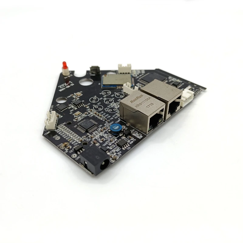
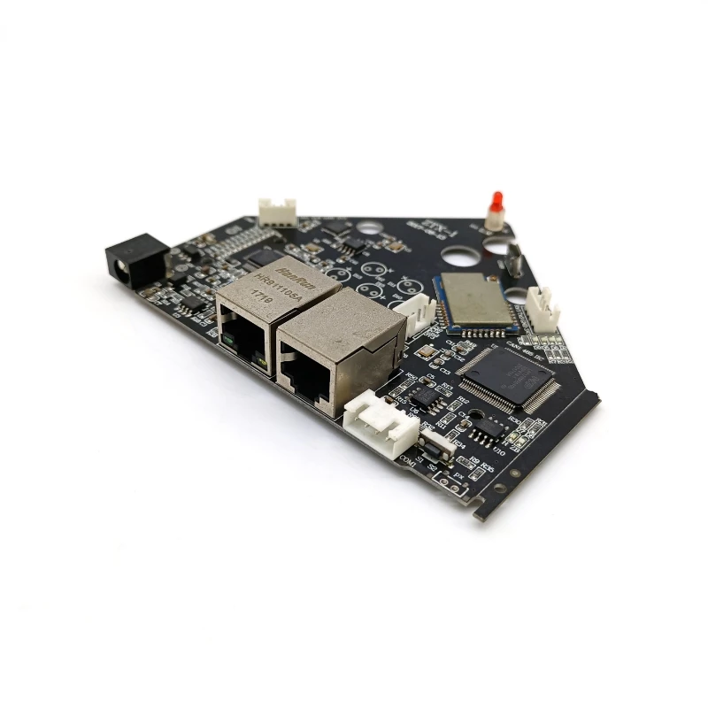
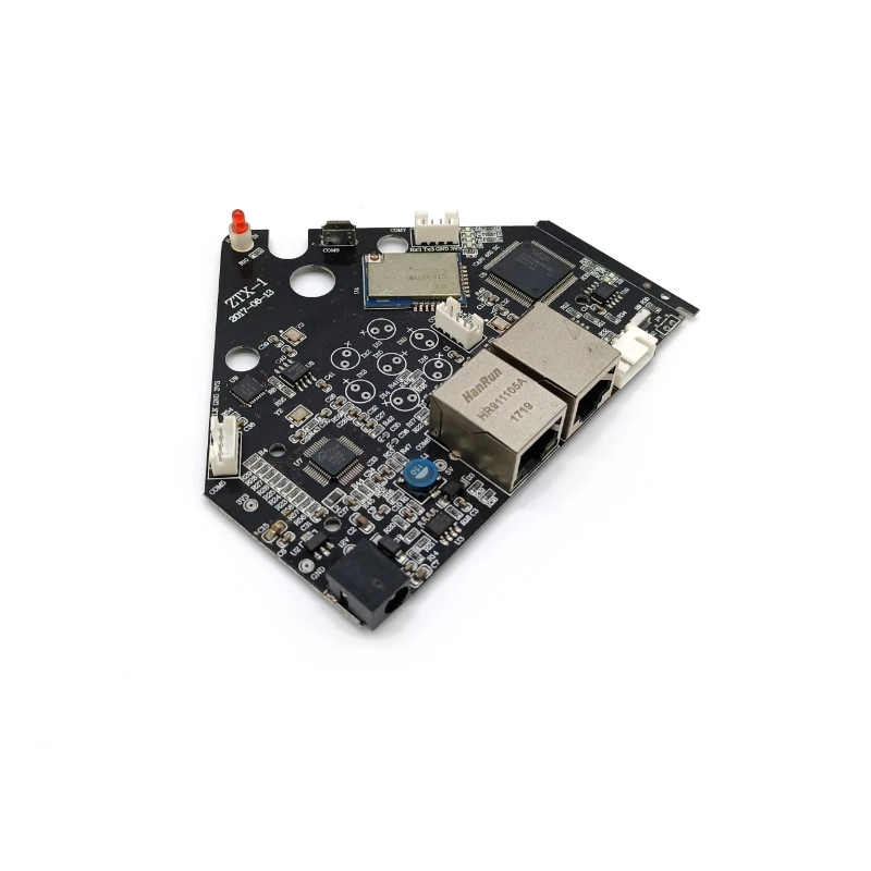
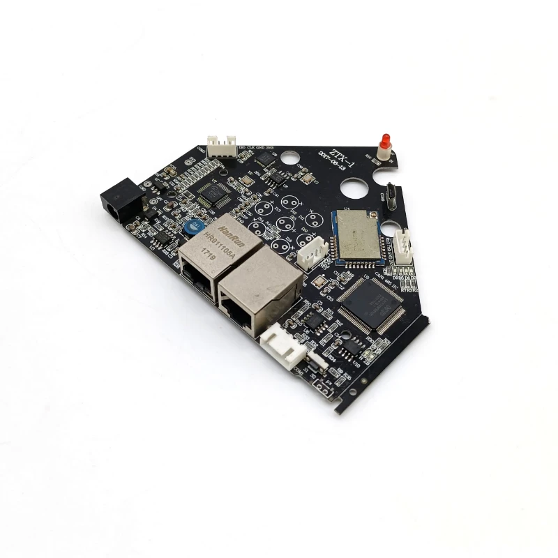
PCB Assembly for Internet and IoT Device
Internet and IoT devices are built around one core expectation — staying connected. Whether the device is sending sensor data, receiving commands, or simply maintaining a stable link to a network, the reliability of that connection depends heavily on the PCB behind it.
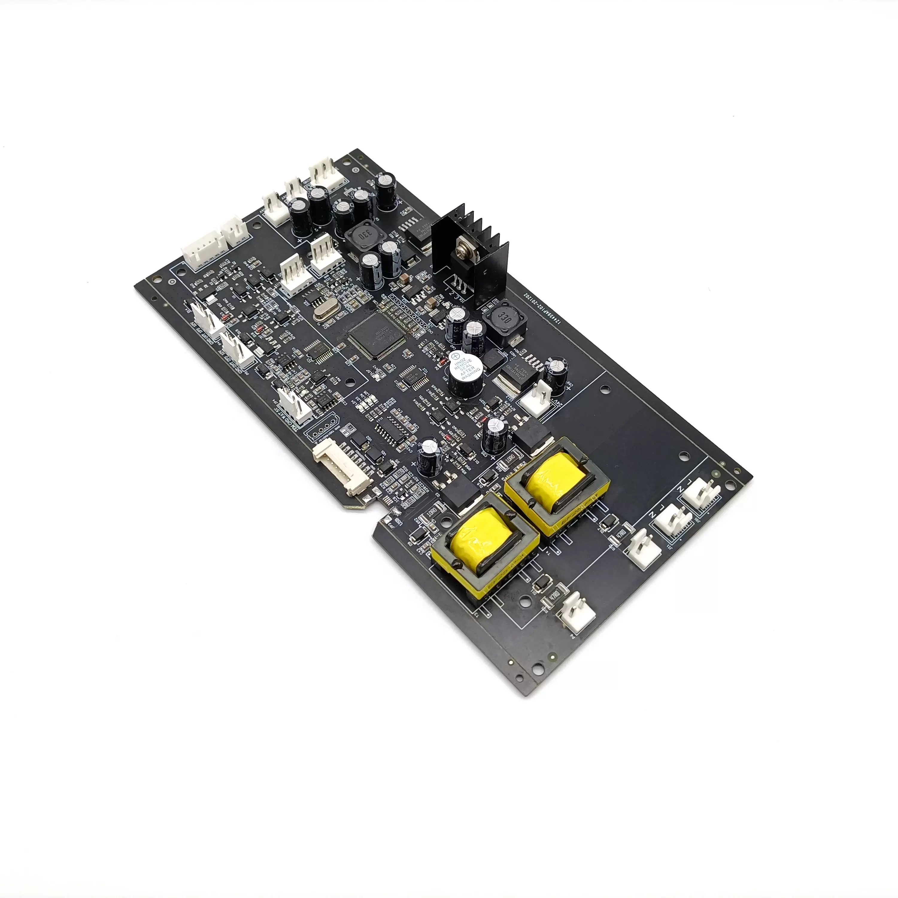
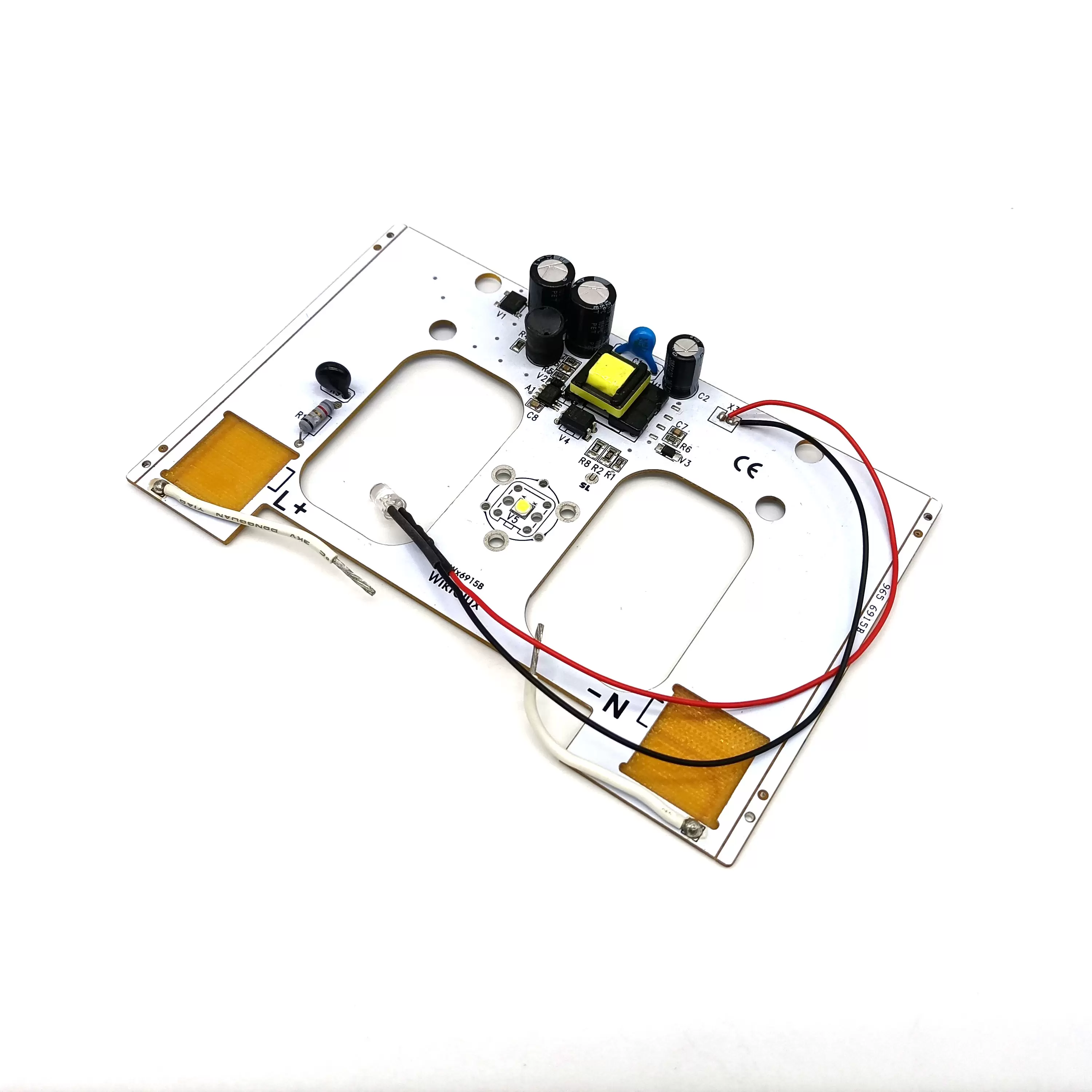
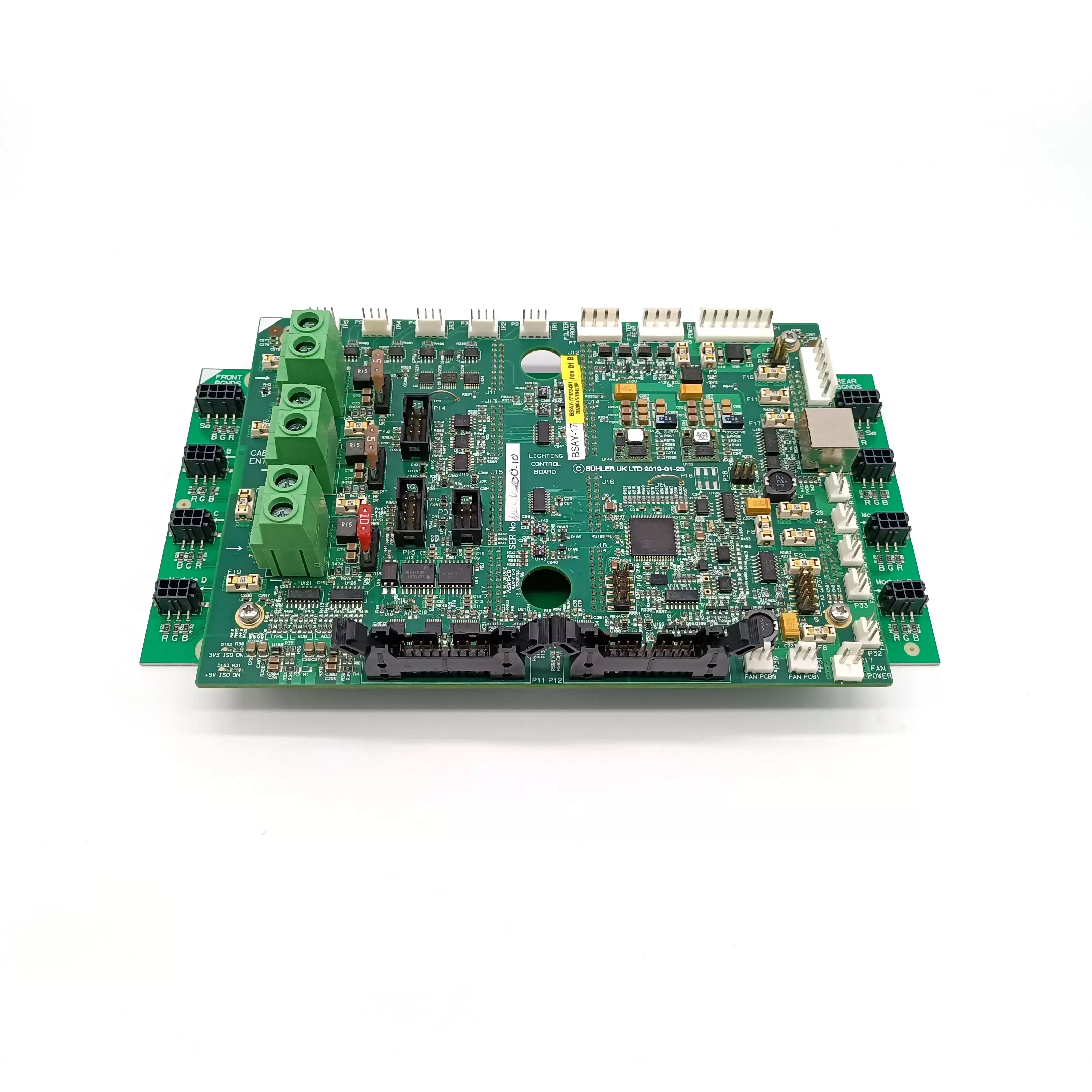
Compared with traditional boards, IoT PCBs often need to handle multiple functions at the same time within a limited space. Communication modules, control units, and peripheral interfaces are integrated onto a single board, which leaves less room for error during assembly. Small variations that might not affect other types of products can lead to unstable connections or inconsistent performance in IoT devices.
At BENLIDA, the assembly process is adjusted to match these characteristics, with more attention given to layout consistency, signal continuity, and overall integration rather than just basic functionality.
Designed Around Connectivity
For IoT applications, performance is often judged by how stable the connection remains over time. A device that frequently drops signals or struggles to maintain communication quickly loses its value, no matter how advanced its features are.
This is why the PCB assembly is approached from a connectivity-first perspective. Signal paths are kept clear and consistent, and the interaction between communication modules and other components is carefully maintained during assembly. The goal is to support smooth data transmission without introducing unnecessary interference or fluctuation.
Working Within Compact Designs
Most IoT devices are designed to be compact, sometimes even constrained to very small enclosures. This means the PCB must carry more functions in a tighter layout, which increases the importance of precise assembly.
Component placement, soldering uniformity, and thermal control all become more sensitive in this context. When everything is closely arranged, even minor inconsistencies can affect nearby circuits. Maintaining balance across the board is therefore a key part of the process, helping ensure that different modules can operate side by side without conflict.
Supporting Low Power Operation
Many IoT devices are expected to run continuously, often with strict power limitations. Some operate on batteries, while others are designed to remain in low-power states for extended periods.
Under these conditions, the PCB needs to behave predictably, especially when switching between active and standby modes. The assembly process plays a role here by ensuring stable electrical characteristics across the board, so that power consumption remains controlled and performance does not fluctuate unexpectedly.
Consistency Across Deployment
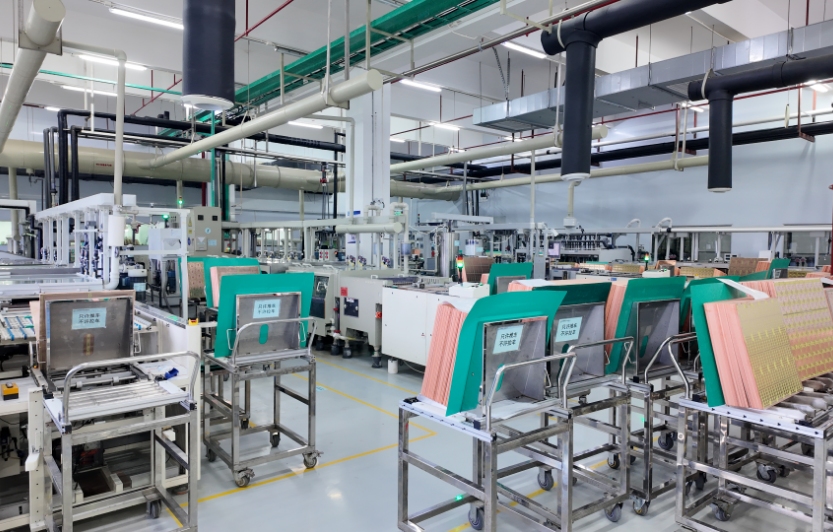
IoT products are rarely built in small quantities. Once a design is finalized, it is usually deployed at scale, sometimes across hundreds or thousands of units. In this case, consistency becomes just as important as individual performance.
If boards from different batches behave differently, it can create challenges during system integration or field use. BENLIDA focuses on maintaining repeatable assembly conditions, so that each unit performs in the same way under the same conditions. This helps reduce uncertainty when devices are deployed in larger networks.
Practical Application Value
In actual use, a well-assembled IoT PCB does not draw attention to itself. It simply allows the device to stay connected, respond as expected, and operate within its intended power range.
For product developers, this translates into fewer communication issues, more predictable behavior, and less time spent troubleshooting hardware-related inconsistencies. Over time, this stability becomes part of the overall user experience, even if it is not directly visible.
PCB Assembly for Internet and IoT Device is built around the real demands of connected products, where communication, control, and power functions operate together on a single compact board. By keeping assembly consistent and well-balanced, it helps maintain stable connectivity, predictable performance, and uniform behavior across devices. This makes it a practical choice for IoT applications that require reliable operation not just in design, but throughout large-scale deployment.

 en
en


 WhatsApp