PCB Assembly for Pogo Pin Carrier
In pogo pin systems, the PCB is not just a circuit—it acts as the interface that determines whether every connection is made correctly, every time.
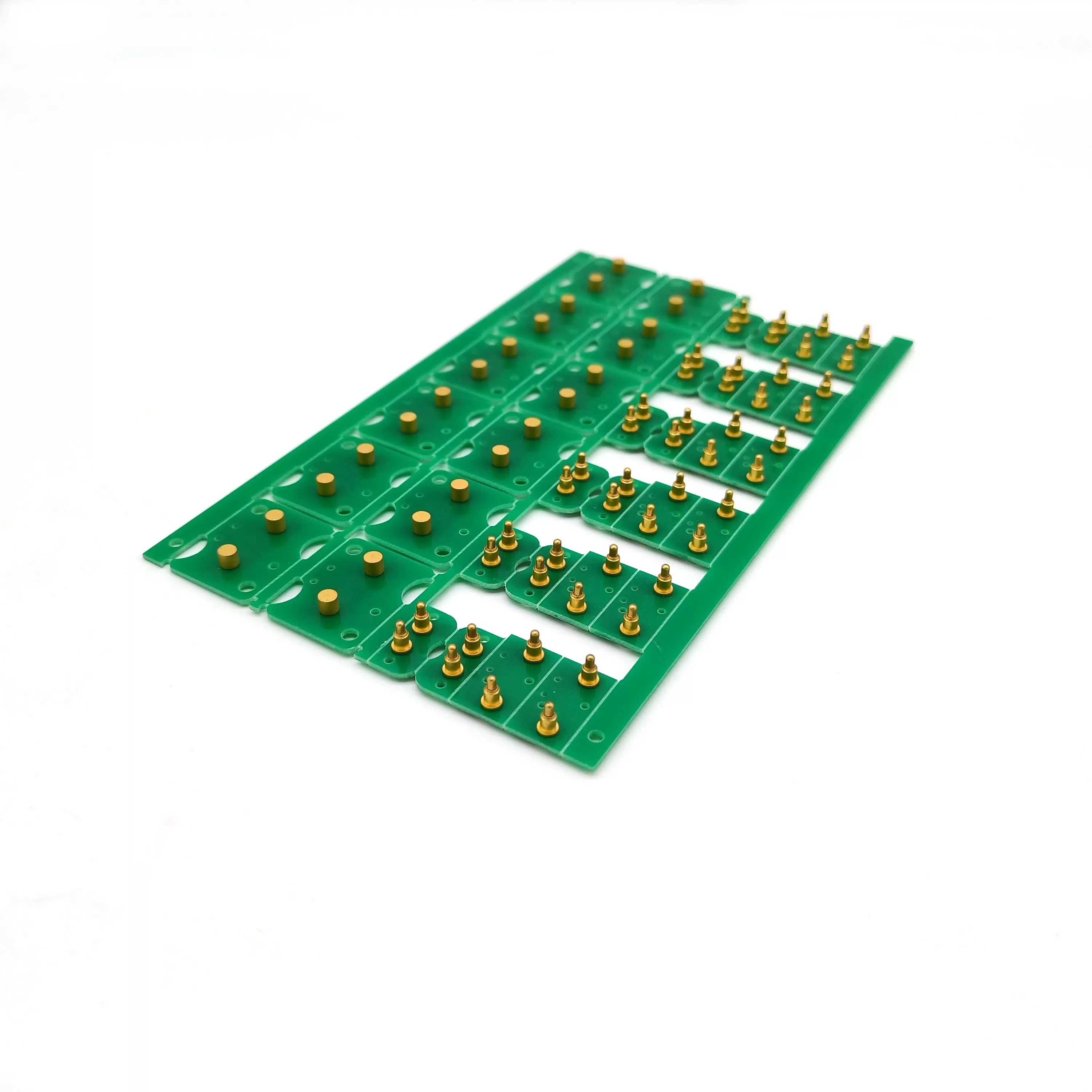
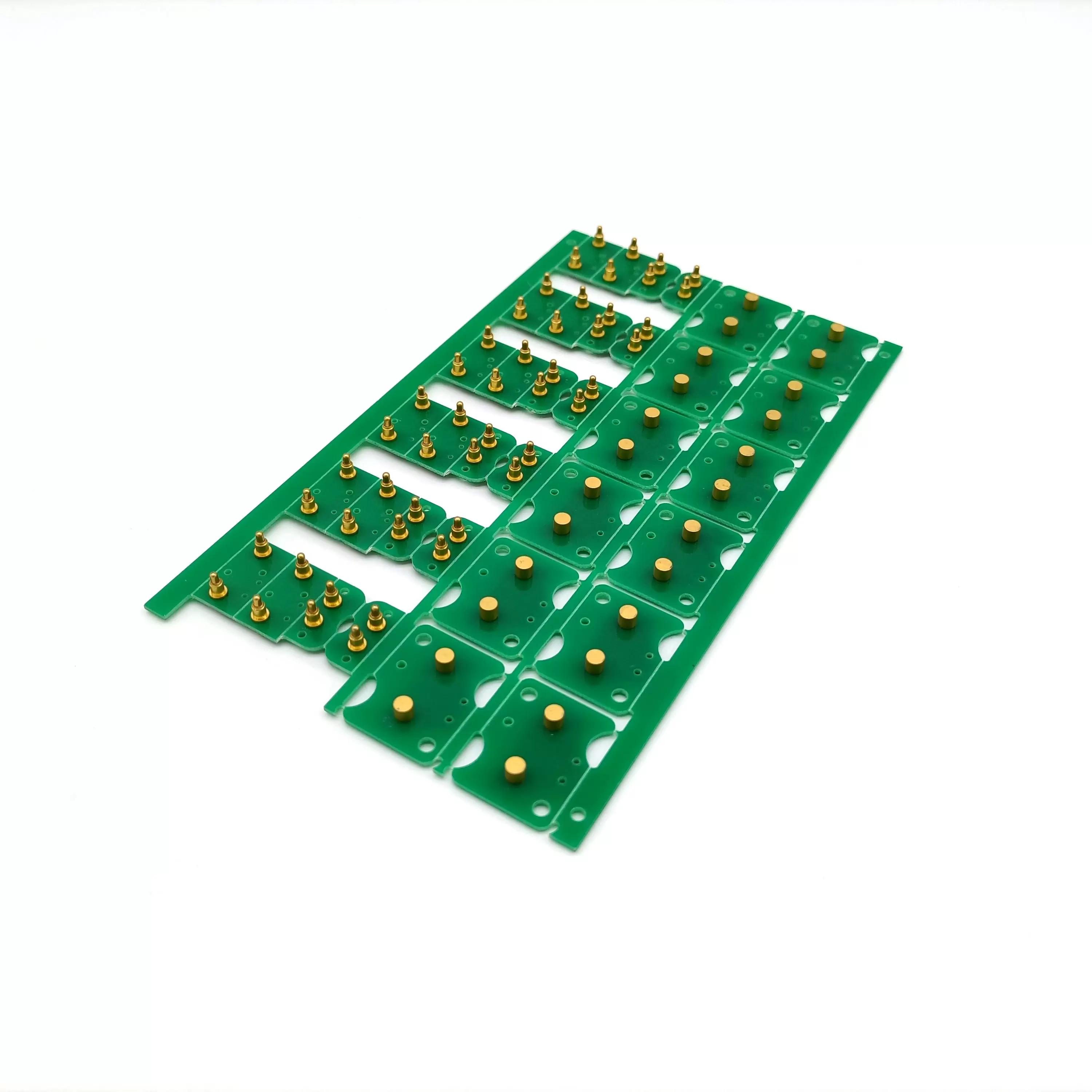
Unlike fixed soldered components, pogo pins depend on physical movement to establish contact. That means the PCB assembly must support continuous mechanical interaction without introducing instability. In real applications, what looks like a simple contact point is actually a combination of positioning accuracy, surface condition, and structural strength working together.
Many connection failures in test fixtures or docking systems are not caused by the pogo pins themselves, but by subtle inconsistencies in the carrier PCB—misalignment, uneven surfaces, or weakened solder joints that only become apparent after repeated use.
What Actually Fails First in Pogo Pin Systems
When a pogo pin interface starts to lose reliability, the failure is rarely sudden. It usually begins with small, almost invisible deviations that accumulate over time.
At the early stage, this might show up as occasional contact instability. As usage continues, the issues become more defined:
●Certain pins require more pressure to establish contact
●Signal transmission becomes intermittent rather than completely lost
●Contact points begin to wear unevenly across the board
●Some channels fail while others continue to function normally
These patterns point to one thing—the PCB is no longer providing a consistent interface for the pins to operate against.
The Role of Flatness and Positioning in Real Use
In theory, pogo pins are designed to compensate for minor height differences. In practice, their tolerance is limited. If the PCB surface is not sufficiently flat, or if pad positioning varies beyond a tight range, the load distribution across the pin array becomes uneven.
This leads to a situation where some pins are over-compressed while others barely make contact.
Over time, this imbalance accelerates wear in specific areas and reduces the overall lifespan of the system. That’s why, in a pogo pin carrier assembly, dimensional control is not just about meeting drawings—it directly affects how forces are distributed during every connection cycle.
Why Mechanical Stress Changes the Assembly Logic
Most PCB assemblies are evaluated under static conditions. Pogo pin carriers, however, operate under dynamic stress.
Every insertion cycle applies force to the same contact points repeatedly. This introduces fatigue not only at the contact surface, but also at the solder joints and copper pads beneath.
If the assembly process does not account for this, long-term issues become inevitable. Solder joints that look acceptable under inspection may gradually develop micro-fractures. Pads may begin to lift slightly, affecting alignment even further.
In this context, assembly is no longer just about electrical continuity—it becomes a question of how well the structure absorbs and redistributes mechanical stress over time.
Contact Surfaces: Where Electrical Meets Mechanical
The interface between pogo pins and PCB pads is where electrical performance is actually defined.
Even with correct alignment, poor surface consistency can introduce variability in contact resistance. Over repeated use, slight differences in surface quality can lead to oxidation patterns or uneven wear, which further affect signal stability.
This is especially important in applications involving data transmission or low-voltage signals, where even small fluctuations in contact quality can have noticeable effects.
How Application Scenarios Change the Requirements
Not all pogo pin carriers behave the same in use. The way the board is integrated into the system determines what matters most.
In test fixtures, consistency over thousands of cycles is the primary concern.
In charging docks, stable contact under slight positional variation becomes more important.
In modular devices, repeated user interaction introduces less predictable mechanical stress.
Because of this, assembly strategies often need to be adjusted—not dramatically, but enough to align with how the product will actually be used rather than how it looks on paper.
A More Practical Way to Look at Assembly Quality
For pogo pin carrier PCBs, quality is not best judged at the moment the board leaves the production line. It’s better understood by how the board behaves after repeated use.
A stable assembly is one where:
●Contact performance remains consistent after extended cycling
●No visible shift occurs in alignment or surface condition
●Electrical behavior does not drift over time
Reaching this level of stability requires not just process control, but an understanding of how mechanical interaction affects electrical performance in the long run.
Closing Perspective
PCB Assembly for Pogo Pin Carrier sits at the intersection of mechanical precision and electrical reliability. It is less about building a board that works once and more about ensuring that it continues to work the same way after thousands of interactions.
When assembly is approached from this perspective, the result is not only a functional interface but a connection system that remains dependable throughout its lifecycle.

 en
en


 WhatsApp