Low output voltage on PCB is a common defects and it's root cause may involve various factors such as input, conversion, control, feedback, then output. Normally it is a systemic problem and cannot be simply attributed to any single component.

Part 1: Detailed Cause Analysis
Analysis Direction 1: (Corresponding to energy conversion/control loop issues) If the voltage is low even under no-load conditions
1. Input Issues
● Low Input Voltage: The AC input voltage itself is insufficient, or the DC input voltage is lower than the requirements.
● Input Filter Capacitor Failure: Capacitance reduced or ESR (Equivalent Series Resistance) increased, will lead to excessive high-voltage DC ripple, affecting the operation of subsequent circuits.
2. Startup and Power Supply Issues
● Startup Resistor Open/Value Changed: The power management IC cannot obtain the initial startup voltage.
● IC Power Supply Circuit Abnormalities: Abnormal output voltage of the IC's Vcc, damaged rectifier diodes, or failed filter capacitors, those may result in insufficient IC operating voltage and weakened driving capability.
3. Feedback Control Loop Failure (Common Causes)
● Value Change of Output Voltage Sampling Resistors: A drift in the value of the voltage divider resistor (usually a precision resistor) connected to the output terminal and leads to incorrect feedback voltage, cause the IC to interpret the output voltage wrongly as "too high" and actively reduce the duty cycle.
● Reference Source Malfunction: Damage or performance degradation of a reference source, such as TL431 results in an inaccurate reference voltage, cause the entire loop reference to be incorrect.
● Optocoupler Failure: Aging of the optocoupler leads to a decrease in current transfer ratio, or complete failure, preventing the feedback signal from being correctly transmitted to the primary side.
● Component Malfunction from Feedback Loop Compensation: Deterioration of compensation capacitors or resistors in the loop will cause loop instability or incorrect response.
4. Control and Switching Issues
● Malfunction on Power Management IC: Damage to the internal reference, error amplifier, or driver section.
● Performance Degradation on MOSFET: Although not completely broken down, the on-resistance Rds(on) becomes extremely high, leading to a significant increase in switching losses and insufficient effective output power.
Analysis Direction 2: (Corresponding to energy transfer/power circuit issues) Sudden voltage drop under load (poor load regulation)
1) Excessive power losses from transfer path
● Losses from switch transistor: Same as above, performance deterioration from switch transistor.
● Malfunction on high-frequency transformer/inductor: Partial short circuits in the windings, core saturation, or changes in the air gap, these factors lead to a severe decrease in energy storage and transfer efficiency, causing a voltage drop when applying a load.
● Performance degradation on output rectifier diode : Increased forward voltage drop (Vf) or longer reverse recovery time, thses factors result in low rectification efficiency and severe heat generation.
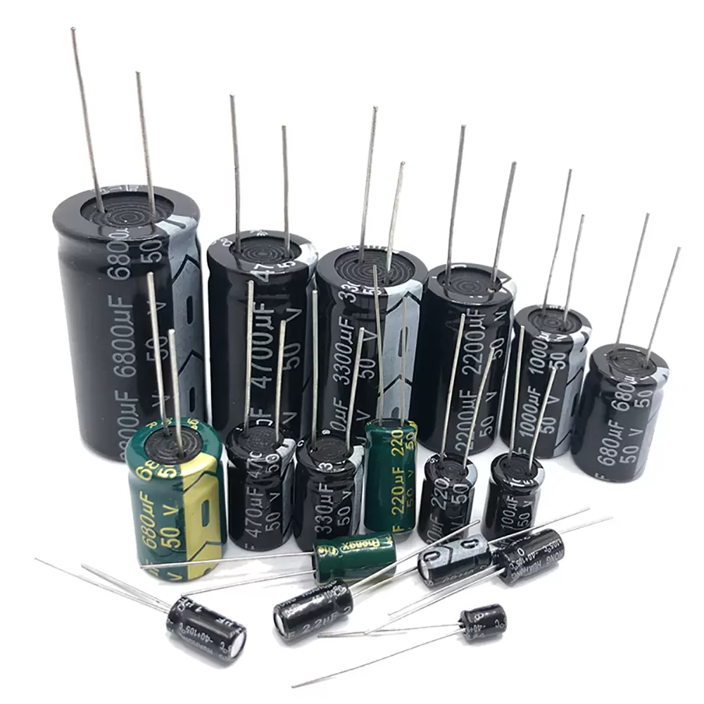
2) Failure on output filter capacitor (extremely common)
● Severely degradation of output filter capacitance or a sharp increase in ESR, these factors prevent it from providing sufficient charge to sustain voltage, during the switching transistor's off-state, result in huge ripple of output voltage and a drop in average voltage under load.
3) PCB and Soldering Issues
● Thin PCB traces, cracked copper foil, or cold/poor solder joints in high-current paths (such as ground and output lines) can lead to excessively high equivalent series resistance and significant voltage drop.
Part Two: Systematic Diagnostic and Troubleshooting Process (Suggested Order)
Step 1: Safety and Basic Confirmation
● Power off! Discharge large capacitors.
● Confirm that the input voltage is within the normal range.
Step 2: Visual and Olfactory Inspection
● Observe is there any burnt components, bulging (especially capacitors), cracks, and poor solder joints.
● Smell is there any abnormal odors.
Step 3: Measurement (Critical Step)
● Measure the voltage across the large input capacitor: Does it reach the expected high-voltage DC?
● Measure the resistance to ground at key points: Check for short circuits at the output; check for breakdowns in the switching transistors and rectifier diodes.
● Measure the feedback loop resistance: Use a digital bridge or precision multimeter, focusing on checking if the output voltage divider resistor value matches the nominal value.
Step 4: Dynamic Measurement After Power-On (Safety Precautions)
● No-load Power-on: Measure the no-load output voltage. If normal, proceed to the next step; if low, focus on the feedback loop and IC power supply.
● Gradual Loading: Use an electronic load, gradually increasing the current from a small amount, and observe the voltage drop curve. If the voltage drops sharply immediately upon loading, focus on checking the output capacitor, rectifier diode, transformer, and power transistor.
● Waveform Measurement (if available with an oscilloscope):
* Switching transistor Vds waveform: Check for saturation or abnormal oscillation.
* Output ripple voltage: Check if the ripple is abnormally large (indicating a failed filter capacitor).
* Voltage across the feedback optocoupler: Check if it changes with the output voltage.
Step 5: Component Inspection(Targeted)
● Capacitor Inspection: Use the replacement method or an LCR meter to measure the capacitance and ESR.
● Diodes/Switching Transistors: Check with a multimeter in diode mode or a dedicated tester.
● Suspected Resistor: Perform precise measurement on the desoldered end.
Summary and Ranking of Common Causes, Based on Probability and Experience:
1. Failure of output filter capacitor (especially electrolytic capacitors) is the number one cause for "on-load voltage drop".
2. Feedback sampling resistor is another common cause of "inaccurate no-load voltage".
3. Performance degradation of rectifier diode, switching transistor, and cold solder joints are also common causes.
Core Mindset&Approach: Follow the energy flow direction of "input → conversion → output", and check one by one along the two main lines of "is the control signal(feedback) accurate".
For low power output voltage issues on PCB&PCBA, professional testing services could be considered as options below:
● Electrical performance testing: Using high-precision power supplies, electronic loads, oscilloscopes, and dynamic analyzers, measure the power supply's load regulation, ripple noise, dynamic response, and switching waveform to quantify the degree of performance degradation.
● Analysis on key Component Parameter: Using LCR meters, semiconductor analyzers, etc., we accurately measure implicit parameters such as capacitor ESR/capacitance, inductance, MOSFET on-resistance, and diode recovery characteristics.
● Thermal Imaging Analysis: Using infrared thermal imagers, we quickly locate abnormal hot spots on faulty boards, providing intuitive clues for fault localization.
● Comprehensive Failure Analysis: We perform electron microscopy, cross-sectional analysis, and material composition analysis on suspected damaged components (ICs, capacitors, transformers) to identify their fundamental failure mechanisms (such as overvoltage, overcurrent, thermal stress, and manufacturing defects).
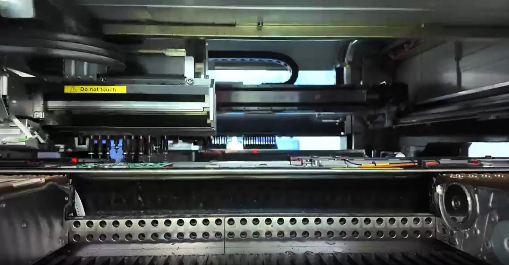
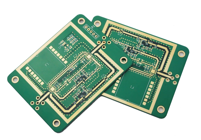
Benlida is a professional PCB manufacturer and also provide PCB assembly service. We follow the trends of the market and customer needs, have built a strong engineering team. In addition to providing production services, we also offer related engineering services. If you are facing complex power supply faults on your PCB and don't know how to solve, or need an analysis report, please contact Benlida!
 en
en

 WhatsApp