In PCBA (Printed Circuit Board Assembly) quality inspection, X-ray inspection is a key non-destructive testing technology, primarily used to detect hidden defects that cannot be detected by visual inspection and electrical testing. This article is going to narrate key applications:
I. Principles of X-ray Inspection
X-rays penetrate the PCBA and different materials have different absorption rates of X-rays (e.g., metals have high absorption rates, plastics/silicon have low absorption rates), forming high-contrast two-dimensional or three-dimensional images on the dispaly such as computor screen, thus revealing the internal structure.
II. Main Inspection Items
1. Soldering Quality Analysis
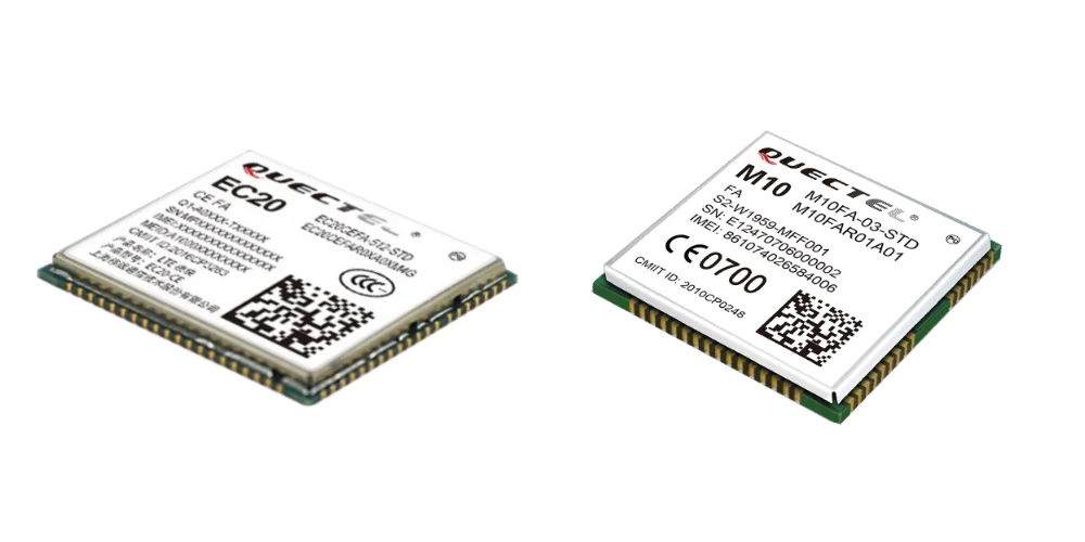
● Hidden solder joints such as BGA/CSP/QFN: Detecting solder ball voids, bridging/short, cold solder joints, misalignment, etc.
● Through-hole soldering: Checking for insufficient solder filler, porosity, and insertion deviation.
● Solder paste printing quality: Assessing the amount and uniformity of solder paste distribution (must be checked before reflow soldering).
2. Internal Structural Defects
● Interlayer Alignment: Misalignment of inner layers in multilayer PCBs.
● Wire/via integrity: Inspect for cracks, breaks, and uneven copper plating on via walls.
● Internal component defects: Such as chip package cracks, poor wire bonding, and voids.

3. Foreign Objects and contamination
● Residual metal debris, fibers, and other conductive foreign objects.
4. Assembly verification
● Component misassembly, omissions, and reverse polarity (identified by shape and internal structure).
● Potential short circuit risk due to insufficient pin spacing.
III. Technical advantages
● Non-destructive imaging: Does not damage the PCBA, suitable for full inspection or sampling.
● High resolution: Micrometer-level identification (e.g., cracks <1μm).
● Automated analysis: With AI algorithms, automatically marks and classifies defects (e.g., void rate calculation).
● 3D CT scanning: Provides tomographic imaging, accurately locating three-dimensional defects.

IV. Typical workflow
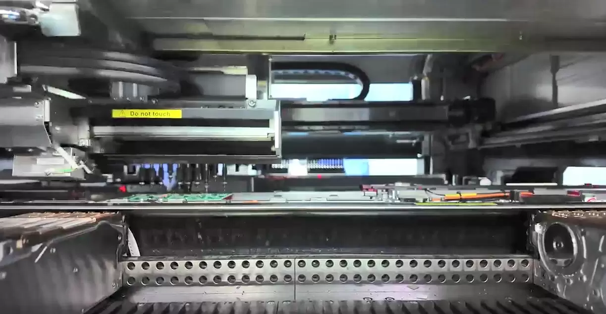
1. PCBA positioning: Place the PCBA on the stage or fixture and set the inspection area&angle.
2. Parameter Settings: Adjust X-ray voltage, current, and focal length according to board thickness and component density of PCBA.
3. Image Acquisition: Obtain 2D projection or 3D scan data.
4. Image Analysis:
● Visual Interpretation: Experienced personnel compare with standard images.
● Automated Software Analysis: Such as measuring solder ball void ratio (IPC standards typically require ≤25%), detecting bridging, etc.
5. Result Output: Generate an inspection report, indicating the location and type of defects.

V. Industry Standards and Specifications
● IPC Standards: Such as IPC-A-610 (Electronic Assembly Acceptability), IPC-7095 (BGA Design and Assembly Process Guidelines).
● Void Ratio Assessment: Typically follows customer specifications or industry practices (e.g., automotive electronics have stricter requirements).
● J-STD-001: Requirements for Soldering Electrical and Electronic Components.
VI. Application Scenarios
● High Reliability Fields: Automotive electronics, aerospace, medical devices.
● High-Density Packaging: Smartphones, wearable devices, microprocessor modules.
● Fault Analysis: Root cause analysis of returned parts.
VII. Limitations
● High Cost: High investment and maintenance costs.
● Inspection Speed: 3D scanning is time-consuming, potentially affecting production cycle time.
● Material Limitations: High-density metal shielding layers (such as thick copper foil) may affect image quality.
● Radiation Safety: Strict management of operator protection and equipment shielding is required.
VIII. Technological Development Trends
● AI and Machine Learning: Automatic Defect Identification (ADI) systems reduce human error.
● Online Integration: Linked with SMT production lines to achieve real-time process feedback.
● High Resolution and High-Speed Scanning: Micro-focus X-ray and rapid CT improve inspection efficiency.
● Multimodal Data Fusion: Combining infrared thermal imaging, ultrasonic data, and other data for comprehensive judgment.
IX. Implementation Recommendations
1. Define Inspection Objects: Define inspection standards based on key product characteristics (e.g., BGA solder joints, automotive ECU modules).
2. Process Integration: X-ray data is fed back to the SMT process to optimize solder paste printing and reflow molding profiles.
3. Personnel Training: Operators must master basic image interpretation and equipment maintenance knowledge.
4. Data Management: A defect database is established for Statistical Process Control (SPC) and quality traceability.
X-ray inspection has become an important process of modern PCBA quality control, especially with the miniaturization and development of high-density electronic components, it's value is prominent. The proper application of this technology can improve product reliability and reduce after-sales risks significantly. Customers and manufacturers need to combine their own product characteristics and quality requirements, balance inspection costs and benefits, and formulate scientific inspection plans.
Benlida is a professional PCB and PCBA manufacturer, continuously invest in advanced equipment and had invested X-ray inspection equipment, provide customers with high-quality PCBs & PCBAs and excellent services continuously that keep up with the latest trends! If your PCBA requires X-ray inspection services, please contact Benlida!
 en
en


 WhatsApp