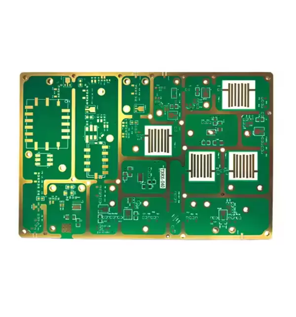
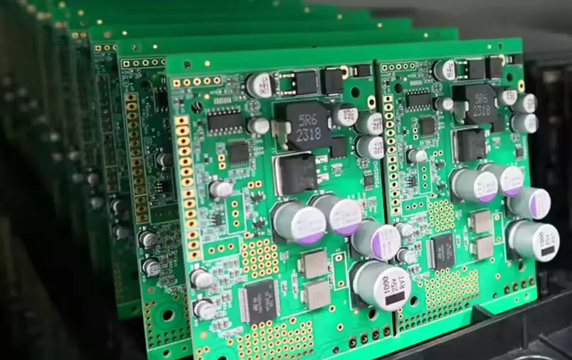
High-frequency PCBs (PCBs) refer to printed circuit boards which working at frequencies above 1GHz, or signal transmission is sensitive to parameters such as dielectric constant and loss factor. Their design, materials, and manufacturing processes significantly differ with other PCBs, and they are primarily applied in radio frequency (RF), microwave, millimeter-wave, and high-speed digital fields.
I. High-Frequency PCB Material
Key characteristics of high-frequency PCB materials are below:
● Low dielectric constant (Dk): Reduces signal delay and increases transmission speed.
● Low loss factor (Df): Reduces energy loss during signal transmission.
● Stable Dk/Df temperature coefficient: Ensures stable performance at high temperatures.
● Low hygroscopicity: Prevents moisture from affecting dielectric properties.
● High thermal conductivity: Facilitates heat dissipation.

Common Applied materials for high-frequency PCBs:
1. Polytetrafluoroethylene (PTFE/Teflon)
● Representatives: Rogers RT/duroid series (e.g., RT5880, RT6002), Taconic TLY/TLE series.
● Features: Dk=2.2~3.5, extremely low Df (0.0009~0.002), but difficult to process with high costs.
● Applications: Millimeter-wave radar, satellite communication, aerospace.
2. Modified PTFE Composites:
● Representatives: Rogers RO3000 series (ceramic-filled PTFE), Arlon AD series.
● Features: Dk=3.0~10, improved mechanical properties, easy to process.
3. Thermosetting Polymer Substrates:
● Representatives: Rogers RO4000 series (hydrocarbon resin + ceramic filler), Isola's IS680 series.
● Features: Dk=3.3~3.7, Df≈0.003, can be processed by traditional technology for FR-4, high cost-effectiveness.
4. Ceramic Substrates (e.g., alumina, aluminum nitride)
● Features: High thermal conductivity, high rigidity, suitable for high-power, high-frequency applications.
5. Special FR-4 Enhanced Version
● Examples: Panasonic Megtron series, Isola FR408HR.
● Features: Specially for high-speed digitals, Df can be as low as 0.005, better cost-effectiveness than PTFE.
II. Key Points of PCB Manufacturing Process
High-frequency PCB manufacturing requires strict control of the following processes:
1. Image Transfer and Trace Width Accuracy
● Use LDI or high-resolution lithography to ensure microstrip trace and coupling trace width tolerances within ±0.02mm.
● Edge roughness might affect signal loss, the etching parameters have to optimize.
2. Dielectric Layer Thickness Control
● The lamination process requires strict control of thickness uniformity, deviations will affect impedance consistency.
3. Hole Metallization
● Plasma desmearing: PTFE materials require plasma treatment to ensure hole wall wettability.
● Chemical copper plating: Use highly active chemicals to ensure complete hole wall coverage.
● Hole filling plating: Hole filling processes are commonly used for high-frequency vias, to reduce parasitic inductance.
4. Surface Treatment
● Immersion Gold (ENIG): Most commonly applied, smooth surface, good for solderability, but be aware of the risk of "black pads".
● Immersion Silver: Slightly lower signal loss, but prone to oxidation.
● OSP (Organic Solder Protector): Only applied in low-requirement scenarios.
5. Solder Mask and Shielding
● Solder Mask Openings: Avoid solder mask covering high-frequency traces, to prevent Dk changes that will affect performance.
● Shielding Treatment: Localized electroplated shielding walls, laser-engraved shielding cavities.
6. Impedance Control
● Apply stripline or coplanar waveguide designs, determine the width/spacing of traces through simulation, and perform TDR testing after PCB fabrication.
III. Applications and Materials
| Application | Typical Applications | Materials |
| Wireless Communication | 5G Base Station Antennas, Filters, Power Amplifiers | Rogers RO4000, RT/duroid |
| Satellite Communication | Spaceborne Transceiver Modules, Phased Array Antennas | RT/duroid, Ceramic Substrates |
| Radar Systems | Automotive Millimeter-Wave Radar (77GHz), Military Radar | RT5880, RO3003 |
| High-Speed Digital | Server Backplanes, 400G Optical Modules, PCIe Gen6 | Megtron 6, Rogers RO4400 |
| Medical Equipment | Medical Microwave Therapy Instruments, Imaging Equipment | Taconic RF-35, RO4003 |
| Testing Instruments | Network Analyzers, High-Frequency Probes | High-Performance PTFE or Composite Materials |
IV. Recommendations
● Frequency <10GHz: Modified epoxy resin (such as RO4000) or high-speed FR-4 can be applied to balance cost and performance.
● Frequency 10-30GHz: PTFE substrate (such as RT5880) but need to pay attention for processing technology.
● Frequency > 30GHz: Ultra-low loss PTFE or ceramic substrates must be applied, and surface roughness must be strictly controlled.
● Hybrid lamination: Apply special materials for high-frequency layers, and FR-4 for low-frequency layers, to reduce and balance costs.
V. Development Trends
● Higher frequencies: Developing ultra-low loss materials with Dk < 2.2 for 6G and terahertz applications.
● Integration: Embedded antenna package (AiP) and embedded technology.
● Thermal optimization: High thermal conductivity substrates (such as Rogers TC series) applied in GaN power amplifiers.
Benlida is a professional PCB manufacturer, for over 14 years, Benlida is dedicated to provide market-oriented, customer-centric service with excellent PCBs, we continuously upgrade equipment and improve production processes. If you need high-frequency PCBs, please feel free to contact us!
 en
en

 WhatsApp