What causes pad lifting during PCB(Printed Circuit Board) and PCBA(PCB Assembly) manufacturing?
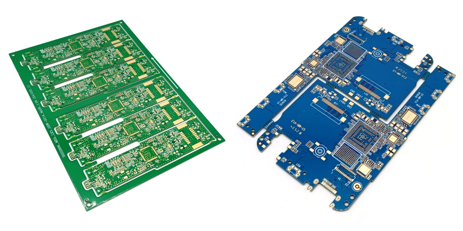
Pad lifting on a PCB is a serious manufacturing defect, manifesting as the copper foil pads separating or peeling off from the substrate (FR-4, etc.) after soldering.
The causes of pad lifting and peeling generally from four categories: poor PCB quality, soldering process misconduct, design defects, and improper operation.
Poor PCB materials and manufacturing defects are the most common and primary causes, and also the most difficult to remedy in subsequent stages
● Poor adhesion between the substrate and copper foil: During the manufacturing process of the PCB substrate (FR-4), the adhesion strength between the copper foil and the insulating substrate is insufficient. This may be due to poor board quality or defects in the lamination process, such as substandard pressure, temperature, or time.
● How to identify: It occurs in regular batches and in multiple locations.
● Poor copper plating quality in through-holes: For through-hole components (DIP), the quality of the copper plating on the hole walls is critical. If the hole walls are rough, with drill debris residue, or the copper plating too thin, it will severely weaken the adhesion between the pads and the PCB.
During soldering, molten solder flows through the hole to the other side. If the plating on the hole wall is not firm, the entire pad will be pulled up.
● Pad damage: During PCB manufacturing, depaneling, or transportation, pads may suffer mechanical damage (such as scratches or abrasions) or external forces such as violent pulling, causing partial separation from the substrate. During soldering, stress concentrates at this point, resulting in pressure separation.
Soldering process issues: Improper soldering operations are a direct cause of pad lifting
● Overheating: Excessively high soldering iron temperatures or prolonged soldering times expose the pads to heat far exceeding their tolerance limits. The resin in the substrate decomposes due to overheating, losing its adhesiveness and causing the copper foil to detach. This problem is particularly common when using high-power soldering irons to solder small pads.
● Thermal shock: Insufficient preheating or direct soldering of cold boards can cause rapid temperature increases, leading to internal stress due to differences in the coefficients of thermal expansion (CTE) between PCB layers, resulting in bonding failure.
● Mechanical Stress
①Moving components during soldering: Moving components or wires before the solder has fully solidified will directly pull on the pads;
②Immediate post-soldering handling: Moving components before the solder joint has cooled to room temperature can also easily lead to pad peeling.
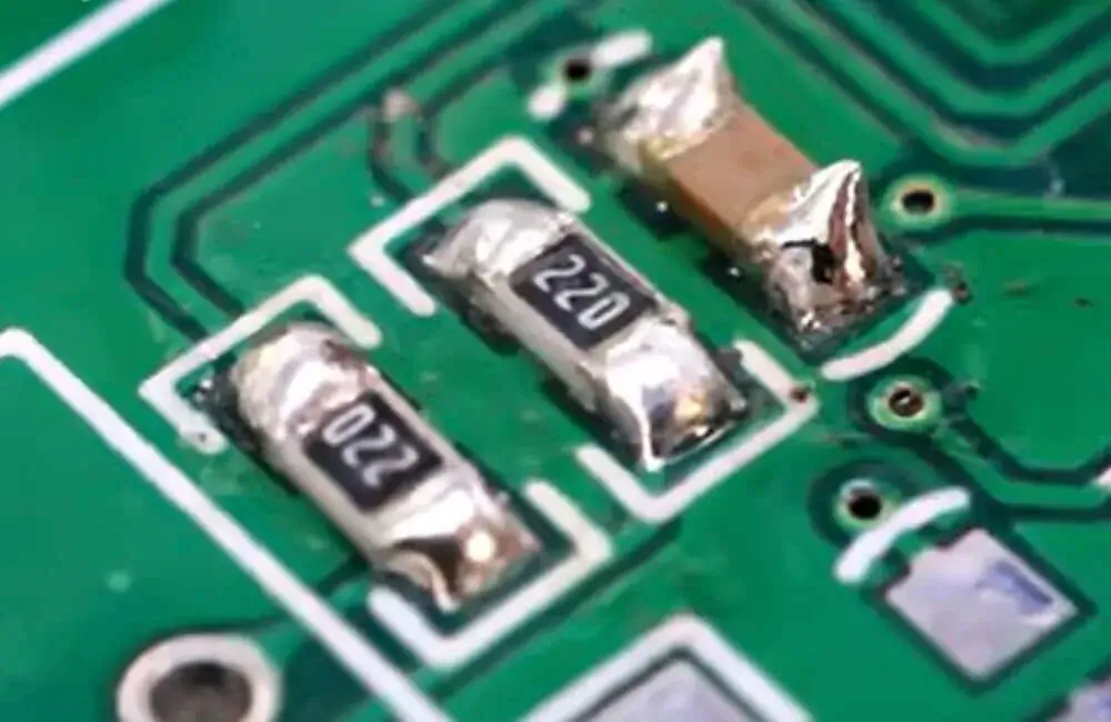
Design and Material Selection Issues
● Inappropriate pad design: Small pads connecting large areas of copper foil (such as power lines) require more heat during soldering, increasing the risk of overheating.
Failure to use teardrop pads for transition leads to stress concentration at the connection between the wire and the pad, making it prone to tearing.
● Thermal stress in multilayer boards: Multilayer boards have complex structures, and the coefficients of thermal expansion (CTE) of different internal materials do not match, resulting in greater internal stress during the thermal cycle of soldering.
● Inappropriate board material selection: Using inexpensive boards with low TG will cause the substrate to soften and decompose once the soldering temperature exceeds the TG value, reducing adhesive strength.
Operational and Rework Issues
● Rough Desoldering: This is a major external cause of solder pad lifting during production. Incorrect angle or excessive force when using a desoldering pump, or excessively high temperature or prolonged use of a hot air gun, can easily damage and detach the solder pads. Forcibly prying components with incompletely melted solder at the bottom can easily tear off the pads.
● Multiple Reworks: Repeated soldering and desoldering cycles on the same solder joint will gradually reduce its bonding strength due to thermal aging, eventually leading to failure and peeling.
How to Avoid and Solve This?
Design
1. Use teardrop solder pads;
2. Avoid connecting large solder pads with thin wires;
3. Select high Tg board material according to process requirements;
4. Manufacturing: Choose a reputable PCB manufacturer to ensure the quality of the substrate material and copper plating process.
Soldering
1. Control soldering iron temperature (320-380℃) and time (<3 seconds/point);
2. Ensure sufficient preheating; use appropriate tools.
Rework
1. Be Patient! Remove components only after fully melting all solder;
2. Use desoldering tape to remove solder, do not prying.
PCB and PCBA Failure Analysis Methods
* Macroscopic and Microscopic Inspection: Use a high-powered microscope to observe the morphology of raised pads and analyze whether it is due to manufacturing delamination, thermal damage, or mechanical damage.
* Cross-Sectioning: Prepare and polish failed pad samples, and observe the interface between the copper foil and the substrate, and the quality of copper plating in through-holes under a microscope. This is the "gold standard" for judging PCB process problems.
* Thermal Analysis: Use thermogravimetric analysis (TGA) to test the Tg value of the PCB board, to examine if it cannot withstand the soldering temperature due to material issues.
* Process Audit and Optimization: Audit the soldering production line, monitor the furnace temperature profile, soldering iron temperature, and usage specifications, and propose process improvement suggestions.
Shenzhen Benlida Circuits Co.,Ltd is a very reliable manufacturer for PCB and PCB assembly, with 14 years of manufacturing experience, we always prioritize quality as first doctrine and insist rigorous quality management. For every project, every PCB, and every PCB assembly process, rigorous process engineering review and supervision are conducted to ensure high rates of good quality and prevent defective products go to customers. If you need PCB and PCB assembly services, please feel free to contact Shenzhen Benlida Circuits Co.,Ltd.

 en
en


 WhatsApp