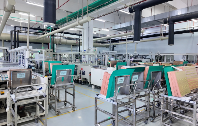
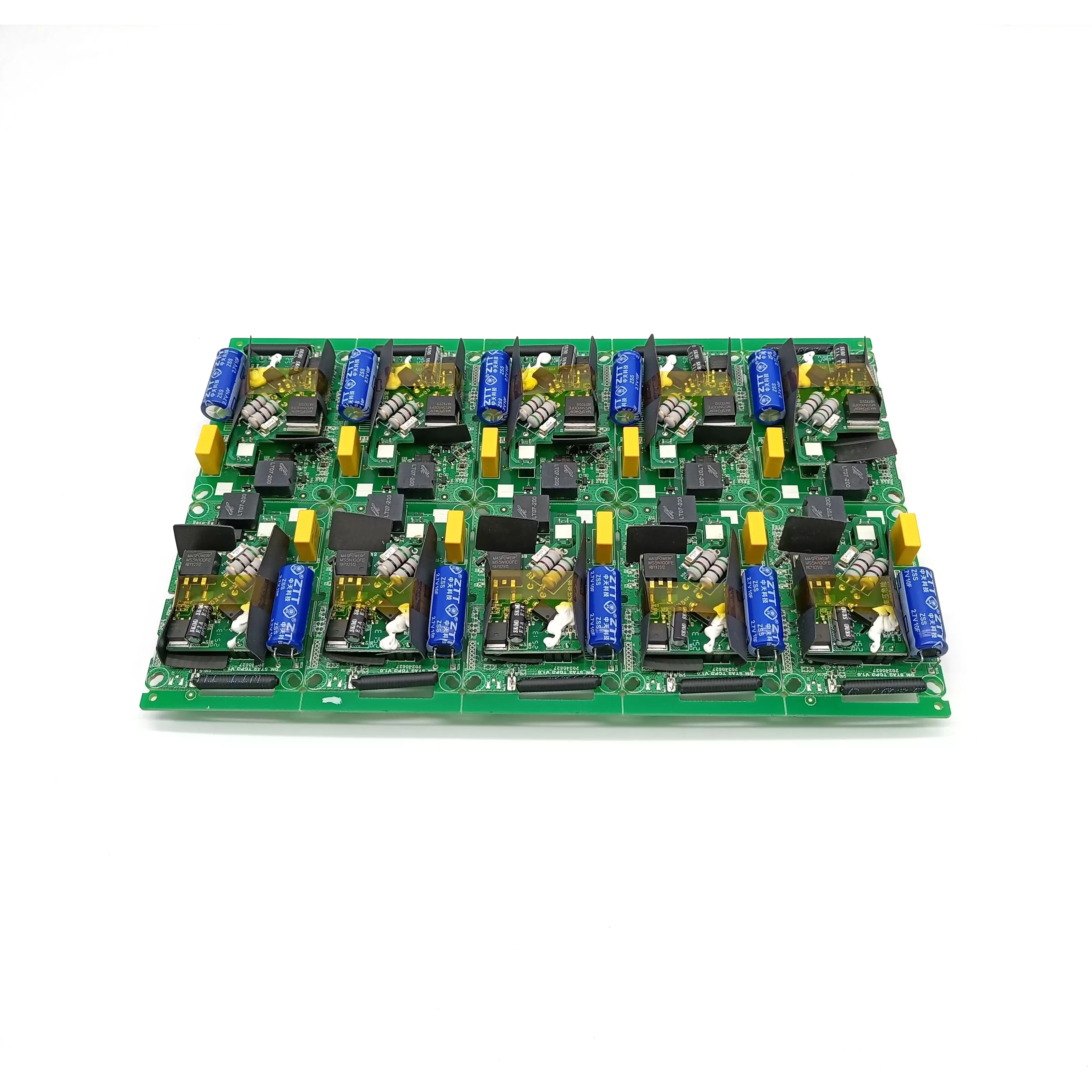
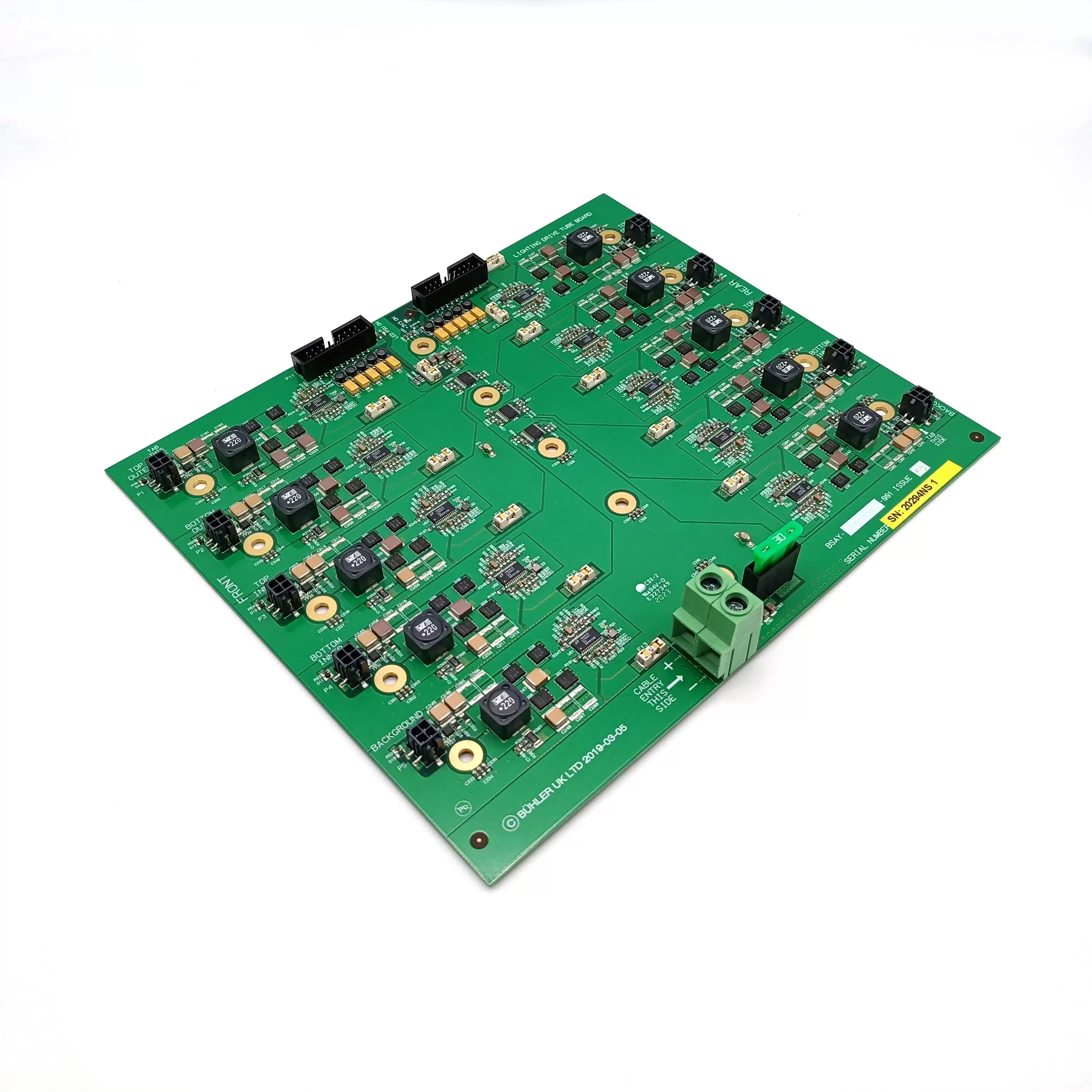
PCB Assembly for IoT Device
We combine top-grade materials with advanced manufacturing equipment to meet the demands of both fast prototypes and full-scale production runs. Each step, from solder paste printing to functional testing, is monitored to ensure the final product meets our high standards.
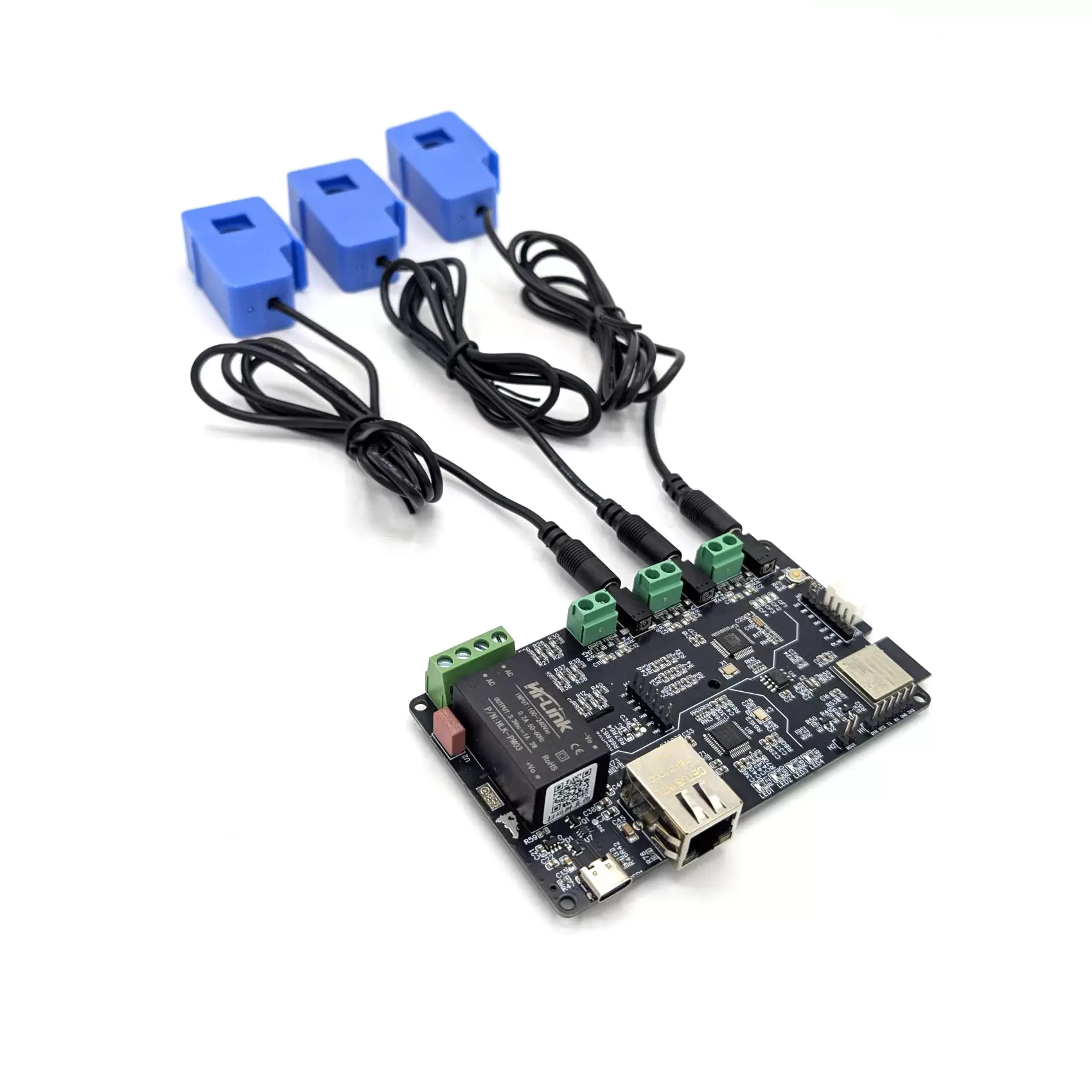
Applications in IoT Devices
Our PCBs are designed to support a wide variety of IoT applications, including:
●Smart Home Devices: Thermostats, smart lighting systems, security sensors — our boards help these devices run smoothly and efficiently.
●Wearables: Fitness trackers, smart watches, and health monitors benefit from our compact, lightweight, and power-efficient assemblies.
●Industrial IoT: Environmental sensors, automation controls, and connected machinery require precision and durability, which our PCBs provide.
●Other IoT Projects: Any device that demands low power consumption, reliable operation, and long lifespan.
Each board is engineered for excellent signal integrity, stable performance across temperature fluctuations, and reliable operation over time.
Manufacturing Process and Equipment
BENLIDA is equipped with state-of-the-art manufacturing technology, including:
●Solder Paste Printing: Precise solder application ensures every component is accurately placed.
●SMT Component Placement: Advanced pick-and-place machines handle even the tiniest and most complex components.
●Reflow Soldering: Lead-free, high-quality soldering ensures long-lasting connections.
●Automated Optical Inspection (AOI): Detects defects early, improving yield and quality.
●X-Ray Inspection: Verifies hidden solder joints for BGAs and other complex packages.
●Functional Testing: Each board is tested to confirm correct operation before shipment.
Whether you need a small batch of prototypes or large-volume production, our facilities can handle boards of varying complexity with precision.
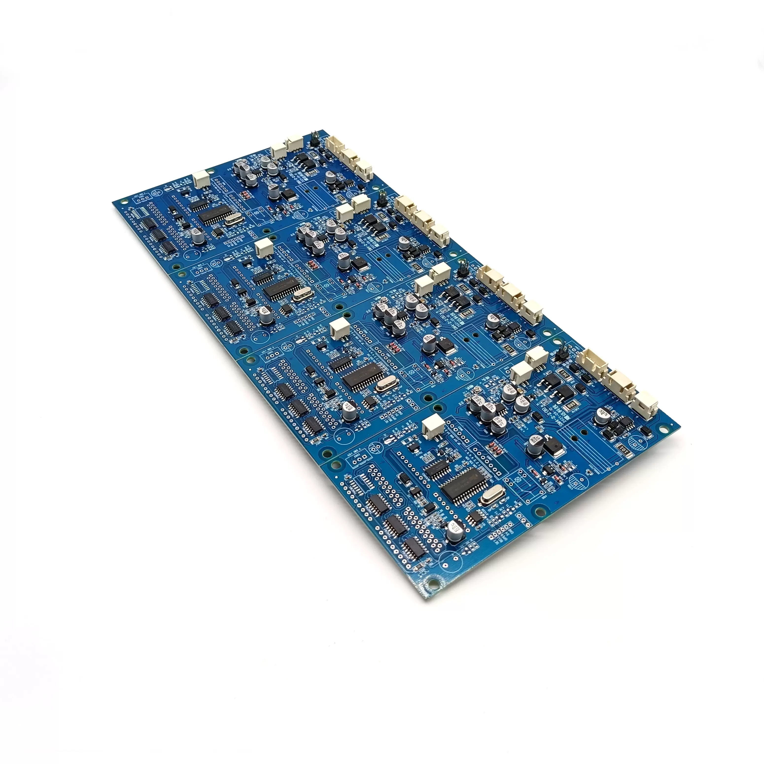
Materials and Technology
We carefully select materials and technologies to ensure top performance:
●FR-4 TG150: Handles high temperatures and provides excellent insulation for reliable signal transmission.
●Copper Thickness 1oz: Supports standard current levels with stable performance.
●Lead-Free HASL Surface: Eco-friendly soldering that ensures long-term reliability.
●Black Solder Mask & White Silkscreen: Enhances visibility for assembly, inspection, and maintenance.
These choices ensure your IoT devices perform consistently in a variety of environments.
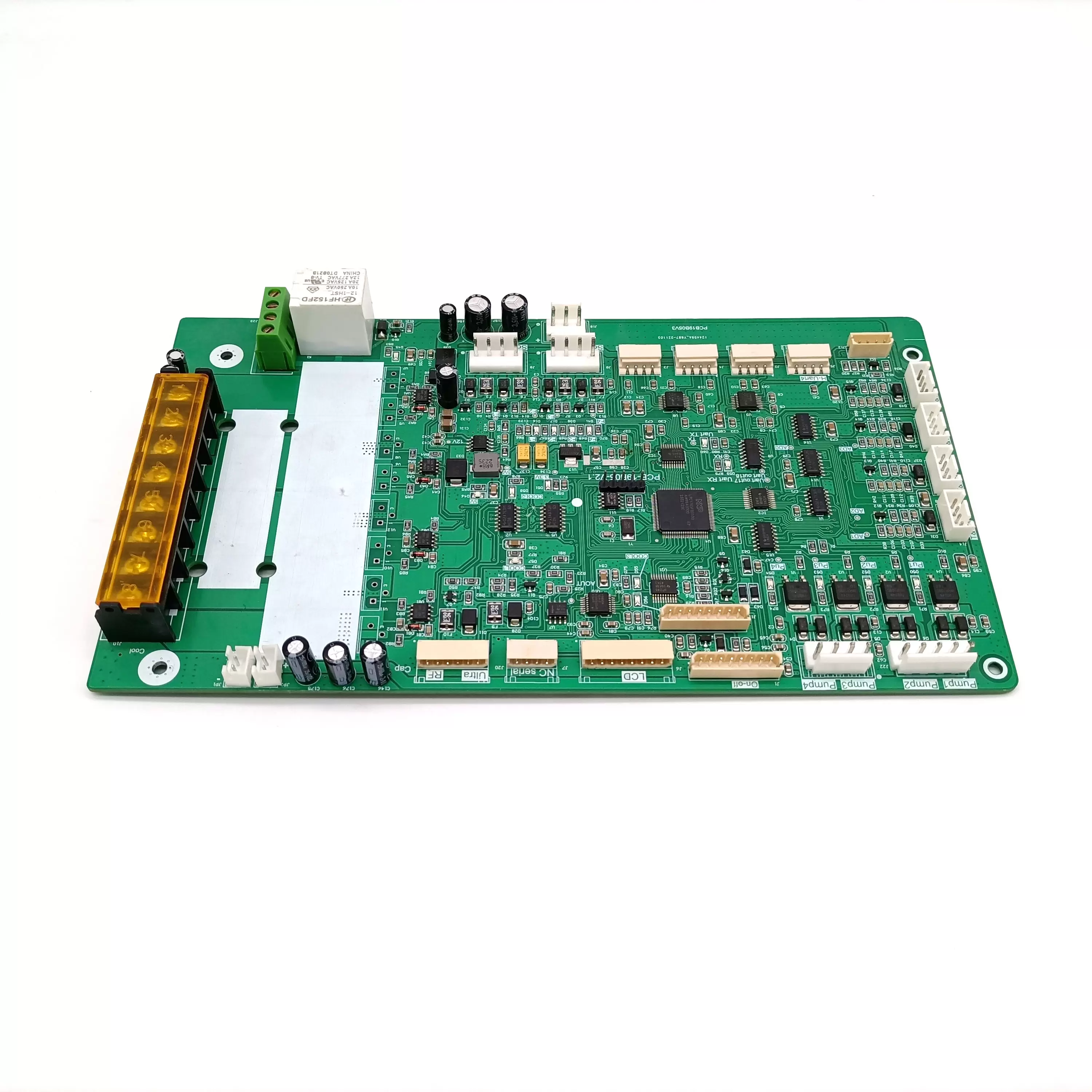
Advantages of BENLIDA PCB Assembly
●High Reliability: Every board undergoes strict quality checks to minimize defects.
●Customizable Solutions: We accommodate a range of sizes, layers, and component types.
●Fast Turnaround: Quick prototypes or large production runs, we meet your timeline.
●Advanced Equipment: Precision machines and inspection systems deliver top-quality assemblies.
With BENLIDA, your IoT project gains reliability, durability, and scalable solutions that adapt as your product grows.
FAQ
Q: Can you assemble multi-layer PCBs for IoT devices?
A: Yes, we support multi-layer boards with high-precision assembly for complex designs.
Q: What is the difference between 1oz and 2oz copper PCBs?
A: 1oz copper is suitable for standard current requirements. 2oz copper can carry higher currents and improves heat dissipation.
Q: How quickly can I receive a prototype?
A: Depending on complexity, our quick-turn service can deliver prototypes within just a few days.
 en
en


 WhatsApp