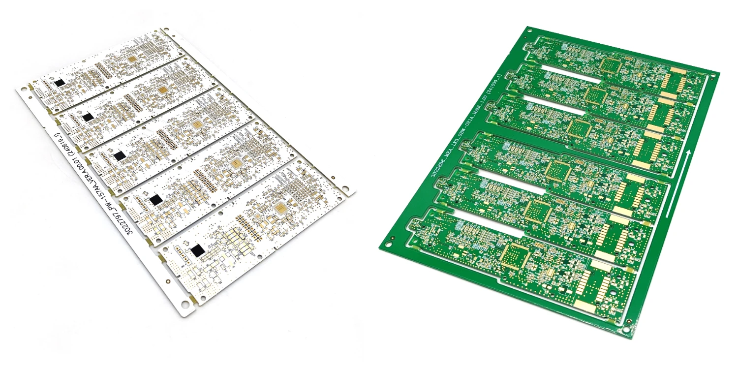
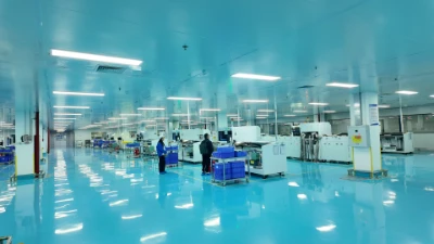
In the electronics industry, PCB manufacturing demands high reliability, consistency, and cost control. Panelization is a technology that combines multiple identical or different small PCB units onto a large board, by using specific connection approaches, such as V-cut and stamp holes. This process brings significant and comprehensive benefits to prototyping, small-batch trial to mass production.
.webp)
Advantages of PCB panelization:
I. Improve production efficiency and equipment utilization (Efficiency)
Efficiency improvement is particularly crucial for prototyping and small-batch production.
1. Improve SMT efficiency significantly: The working efficiency of equipments, such as solder printers, pick-and-place machines, and reflow ovens is commonly calculated as per "board." Panelizing 10 small boards into one large board, it means that could complete soldering progress of 10 boards in one operation. The time spent on equipment such as changeover, alignment and transportation, could be distributed evenly to each small board, shortening the overall production cycle significantly.
2. Simplify Post-Processing: For common circuit board processes, such as conformal coating, selective soldering, and functional testing, panelization support for batch processing, avoid the tedious work of handling each individual board and improve the consistency and efficiency of subsequent processes.
II. Reduce Overall Costs Significantly(Cost): For cost-sensitive projects, panelization could reduce costs at multiple stages.
1. Divide Overall Costs: PCB factories charge engineering fees, mold fees, test fixture fees, and set-up fees, based on the "large board." Panelization maximizes the application of board dimension, reducing the average engineering cost per board effectively.
2. Reduce Material and Logistics Costs: Purchasing, warehousing, and transporting in "large board" units is more efficient than managing numerous small boards, it reduces material coding, inventory, and the risk of incorrect materials, thus lower the management work and logistics costs.
III. Ensure Process Consistency and Reliability (Quality): The core of quality is stability and reliability, and panelization provides process assurance for this.
1. Consistent Process Environment: All boards on the same panel going through same printing, surface mount, reflow soldering, and cleaning processes, minimize the process variations between each ones. It provides a fair and consistent benchmark for reliability comparison and performance.
2. Enhance Test Coverage and Testability: Standardized test points can be designed, support batch electrical testing of the entire panel, by automative testing equipment. Furthermore, the panel is easier to install and monitor during reliability tests such as vibration and temperature/humidity cycling.
IV. Optimize Supply Chain and Production Management (Management)
1. Simplify Supply Chain: the management work for material procurement, production could reduce significantly when combine several units onto one panel.
2. Traceability and Prevent Mistakes: Adding board codes, version numbers and QR on panel could help to prevent mistakes during procurement and production, it also prevents mixing of components for panels.
Regarding electronic characteristics and specific considerations, the following points must be carefully considered during panelization:
1. Reliability Verification: In vibration, shock, and temperature cycling tests, the panelization must ensure that connection(such as micro-bridges in V-cuts and stamp holes) does not experience stress concentration during testing, thus affecting the reliability conclusions of individuals.
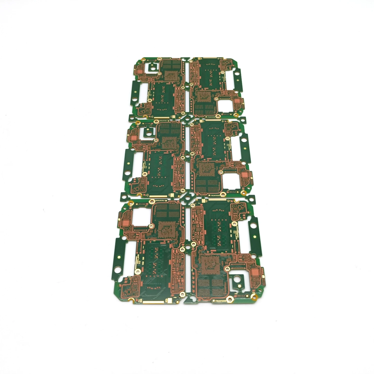
2. Separation Methods: The separation methods must be based on the board materials (e.g., high-frequency materials, thick copper plates) and requirements for framework precision: V-cut (straight-line separation, high efficiency, but may cause burrs) or stamp holes (complex shapes, more stress dispersion, but may leave bumps).
3. Process Edge: Sufficient process edges must be added on the panelization, for clamping, positioning on SMT equipment. Optical positioning points, test points, and breakaway tabs should be on the process edges as well.
Core Advantages of Panelization:
1. Increase efficiency;
2. Reduce cost;
3. Guarantee consistency;
4. Simplify management;
Conclusion:
For printed circuit board/PCB manufacturing, panelization is a highly cost-effective and strategic engineering approach. This is not only about cost savings, but also a key driver to improve efficiency, ensure product consistency, and accelerate the final product development process. Of course, communication between R&D team and PCB manufacturer is important during production, consideration for the panelization method, process edges, and reliability requirements.
Benlida's services include:
1. Production of printed circuit board and assembly(SMT&DIP) service;
2. Engineering service: PCB manufacturability review, evaluatation for panelization approaches (includes connectors, process edges, and layout), and provides optimization suggestions that meet reliability requirements;
3. Process reliability testing: Performing thermal cycling, mechanical shock, vibration, and bending tests, to evaluate the reliability of the panelization and individual boards after panelization;
4. Functional Testing for printed circuit board/PCBA;
5. Failure analysis: Provides analysis service for quality issues, such as solder cracking, solder mask detachment;
6. Materials and processes: Provides relevant qualification documents for the substrates, inks, and soldering processes.
If you are going through research and development for electronic project, and need printed circuit board/PCB manufacturing services, please feel free to contact Benlida. With our professional manufacturing and engineering capabilities, we provide high-quality services for your products from prototyping to mass production!
 en
en


 WhatsApp