Copper plating is one of critical processes of PCB manufacturing, it decides the copper thickness, integrity and connectivity on vias/hole walls. This defect is most fatal issue on PCB, impact the performance and reliability significantly. Plating defects are mostly caused during manufacturing process, below are common causes and negative influences on PCB and assembled PCB/PCBA:
I. Main Causes of Copper Plating Defects
1. Improper Pretreatment
- Cleaning: Residues, oxides, dust, even burs, glass tissues on the hole surface, leads to poor adhesion or interruption of the plating.
- Insufficient Micro-etching: roughness of the copper surface decides the adhesion of the plating, when the roughness is not sufficient, it leads to weak adhension and fallen of plating.
- Poor Activation: The activator fails during copper plating, resulting in discontinued weak plating.
2. Electroplating Process Issues
- Current Density: If current is too high, it could lead to "burnt" and rough plating, and too low would result to thin, uneven and weak plating.
- Imbalance of Plating Fluid:
Low Concentration of Copper Ion: Slow plating speed, thin plating on the hole walls.
Additives Imbalance: Failure of gloss agents and leveling agents, would lead to a dark plating and rough plating.
- Contamination: Organic impurities (oils), inorganic impurities (metal ions), or floating elements, they impact the quality of the plating.
3. Temperature and Chemical Balance:
Unstable temperature or un-balance of chemical substances, cause the uniformity and uneven of the plating.
4. Physical issues which impact the plating
Rough Hole Walls
Drilling Residues
Moisture Absorption
Contamination on the substrates
5. Equipment and Operational Factors
Anode problems: Improper phosphorus copper anode ratio or passivation would lead to fluctuations of the copper content in the plating fluid.
Poor fixture contact: Uneven current causes uneven on plating thickness.
Malfunction of filtration system : Impurities in the plating fluid are not removed in time.
6. Environment and Water Quality
Dusts: Dusts which floating in air, fall into the plating fluid or on the board surface, impact the plating surface.
Impuric water: Impurities in the rinsing water could contaminate the plating fluid.
II. Negative Influence of Copper Plating Defects
1. Decrease Electrical Performance
Poor conductivity: Thin, poor copper or voids in the holes would increase resistance, increase the interruption on signal transmission.
Risk of short circuit: Copper nodules may cause shorts on adjacent lines.
2. Reduce Mechanical Reliability
Poor Adhesion: Blistering and falling of the plating will affect the adhesion of plating on walls.
Hole Wall Fracture: Uneven or excessively thin copper in holes, could cause cracking when under thermal and temperature changes.
3. Degrade Signal Integrity
Impedance Control Failure: Uneven plating could impact impedance, cause reflection and attenuation for high-speed signals.
Degrade High-Frequency Performance: Rough plating increases "skin effect" losses.
4. Soldering and Assembly Issues
Poor Soldering: Oxidized or rough plating will impact solder wetting, leading to cold solder joints.
More Issues in following processing: Poor plating hinders solder processes and cause more risks during repair.
Pad Detachment: Poorly bonded plating might peel off during reflow soldering.
5. Long-Term Reliability Risks
Accelerating Corrosion: Porous or thin areas of the plating would corrode easily, faster, leading to circuit failure.
Thermal Management Failure: Plating defects will impact heat dissipation, accelerating device thermal fatigue.
6. Appearance Issues
Appearance Defects: Darkening, spots, and uneven surface, would decrease the outlook of the boards.
III. Key Approaches to Prevent Defects
Pre-treatment: Enhance cleaning, micro-etching, and activation control.
Monitor Plating Fluid: Monitor the fluids regularly and adjust the composition timely, and filter regularly to remove impurities.
Optimize Electroplating Parameters: Keep current density, temperature, and stirring conditions stable.
Equipment Maintenance: Inspect anodes, fixtures and filtration systems regularly and react immediately if anything beyond certain rules and requirements.
Environmental Control: Keep clean the workshop and keep the water pure.
Analyzing the root causes systematically and implement management, copper plating defects could be significantly reduced, decrease PCB yield rate and improve product lifespan. In production, it is recommended to perform investigations, according to the specific defects, such as voids, crack, thin plating, etc.
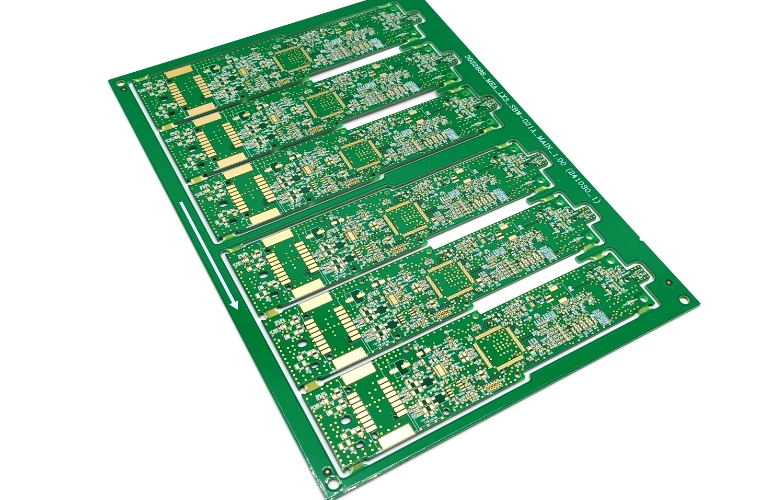
Benlida specializes in PCB manufacturing for 14 years, relying on advanced copper plating equipment and a professional team of engineering&quality, we optimize production processes continuely and control processes with rigorous rules®ulations. Pursue excellence and safeguard the quality of every piece of PCB.
If you and your PCB confront issues, such as decreased electrical performance, poor conductivity, broken via walls, impaired signal integrity, detached pads, or apperance defects, please contact Benlida for consult and technical support!
 en
en


 WhatsApp