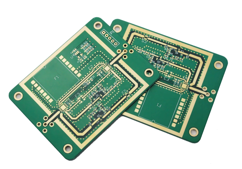
If you’re evaluating a PCB Fabrication Service, solder mask is one of the fastest “tell me how you build” checkpoints in the PCB manufacturing process. On the surface, it looks like a colored coating. In reality, solder mask on PCB is a precision photolithography step that controls where solder can—and cannot—go, protects copper from oxidation, and helps keep fine-pitch assemblies stable through reflow and years of service.
This guide explains how is solder mask applied in real production: materials, coating and imaging steps, tolerances, DFM rules, via treatments, common failure modes, and how to specify mask correctly so your boards assemble cleanly the first time.
1. Why Solder Mask Application Matters More Than You Think
Solder mask is both an electrical insulation layer and a process control layer. A good solder mask process:
Improves assembly yield by preventing solder bridges, especially between fine-pitch pads.
Protects reliability by reducing corrosion, moisture attack, and ionic contamination exposure on copper.
Stabilizes fine-pitch performance by keeping solder volume and wetting behavior consistent during reflow.
Supports long-term durability by resisting cracking, peeling, and chemical attack through handling and cleaning.
A common misconception is “it’s just green paint.” But modern solder mask is usually a photoimageable polymer applied to a controlled thickness, patterned with UV exposure, chemically developed, and fully cured—very similar in concept to how circuit patterns are imaged and etched.
What you’ll learn:
What solder mask does (and does not do)
Material types (LPI vs dry film vs epoxy)
The PCB solder mask process step-by-step
Thickness, clearance, registration, and via rules
Defects, root causes, and practical prevention
How to call out solder mask correctly in design files
2. What Is Solder Mask on a PCB?
2.1 Definition and Core Functions
Solder mask on PCB is a protective dielectric coating applied over copper circuitry, leaving openings only where soldering or electrical contact is needed (pads, test points, certain via types).
Core functions:
Electrical insulation: reduces accidental shorts and leakage risk, especially on dense routing.
Solder bridge prevention: stops solder from wetting unintended copper areas during assembly.
Oxidation protection: shields copper from air exposure, improving long-term stability.
Chemical & moisture resistance: helps resist flux residues, cleaning agents, and humidity.
2.2 Solder Mask vs Conformal Coating
These are often confused, but they solve different problems.
Solder mask is applied during PCB fabrication, patterned by imaging, and primarily controls solderability and protects copper.
Conformal coating is usually applied after assembly (PCBA), covering components and solder joints to protect against moisture, dust, and harsh environments.
Key differences:
Coverage: solder mask is selective (pads are opened); conformal coating usually covers almost everything unless masked off.
Thickness & purpose: solder mask is a fabrication dielectric; conformal coating is an environmental barrier.
3. Materials of Solder Mask Applied in PCB Manufacturing
3.1 LPI Solder Mask (Industry Standard)
LPI solder mask (Liquid Photoimageable) dominates modern fabrication for a reason: it balances resolution, throughput, and durability.
Why most modern boards use LPI:
Good resolution for dense SMT
Compatible with automated coating lines
Strong adhesion and chemical resistance when processed correctly
Typical traits:
Liquid polymer system applied by spray or curtain coating
UV-imaged through a phototool (or via direct imaging)
Developed to open pads and vias
Final thermal cure for chemical/thermal stability
3.2 Dry Film: Photoimageable Solder Mask
Dry film solder mask is laminated as a film, then imaged and developed.
Why it is widely applied:
● Excellent at thickness uniformity
● Good for certain high-density needs where the thickness of consistent dam matters
● When very rigorous requirements for mask
Trade-offs:
● Lamination might struggle over aggressive topography
● Process windows can be less forgiving on rough surfaces or uneven copper
Epoxy solder mask (screen printed, non-photoimageable) is older and simpler.
Where it still appears:
Low-density boards
Some quick prototypes
Cost-driven applications where fine features are not required
Limitations:
Lower resolution and less precise pad definition
More variability in thickness and edge quality
Not a great match for fine-pitch or tight mask dams
3.4 Special Solder Masks
Flexible PCB solder mask: may use polyimide-based coverlays or flexible photoimageable materials designed for bending.
High-temperature solder mask: formulated for elevated thermal stress, automotive, or harsh processing.
UV-curable / inkjet-applied mask (emerging): can reduce phototool dependency and improve agility for some workflows.
4. Step-by-Step: How Solder Mask Applied on PCB
Below is the practical PCB solder mask process most fabrication lines follow. Small variations exist by material, equipment, and board type, but the logic is consistent.
4.1 Surface Preparation (Critical but Often Ignored)
Before coating, the copper surface must be prepared to bond reliably.
Typical steps:
Cleaning: remove fingerprints, oils, and processing residues
Micro-etch: lightly roughen copper for mechanical adhesion
Activation: chemical or plasma treatment depending on process
Why this stage is make-or-break:
Poor prep is one of the top causes of mask peeling, undercutting, and delamination after reflow.
Contamination can cause pinholes or weak ad
4.2 Solder Mask Coating Methods
Once clean, mask is applied using one of several methods:
Spray coating: good for uniform coverage on complex topography
Curtain coating: high throughput and consistent film build on flatter panels
Screen printing: legacy method, still used for some lower-density needs
Thickness control (conceptually):
Coating starts as a wet film.
After tack cure and full cure, it becomes a dry film with a stable final thickness.
The goal: enough thickness for insulation and durability, but not so much that it floods fine features or causes slivers.
4.3 Soft Bake / Tack Cure
This step partially dries the coating:
Drives off solvents
Stabilizes the film so it can be handled and imaged
Helps prevent flow or sag during alignment/exposure
If tack cure is too short, the film may deform during imaging; too long, and it can become harder to develop cleanly.
4.4 UV Exposure (Photolithography)
This is where “paint” becomes “pattern.”
● A phototool (or direct imaging system) defines which areas will remain as solder mask and which will open as pads/vias.
● Alignment uses fiducials and registration targets to align mask openings precisely to copper pads.
Outcomes depend on the material system, but the practical outcome is the same: openings on pads must be cleanly with accurate edges.
4.5 Development (Opening Pads and Vias)
Panels go through a developer (often alkaline) that removes the intended areas and creates:
pad openings
via windows (if vias are not tented)
clearance around features based on defined expansion rules
This step must balance:
clean pad definition (no residue)
minimal undercut
stable dams between pads
4.6 Final Thermal Cure
Final cure locks in:
chemical resistance
heat resistance for lead-free reflow
adhesion strength
long-term stability against cracking
A well-cured solder mask should tolerate assembly heat cycles without softening, blistering, or becoming brittle.
4.7 Inspection and Touch-Up
Inspection looks for:
misregistration
pinholes
mask slivers
pads partially covered
unexpected openings or blocked vias
Tools and methods:
Visual inspection + magnification
AOI (Automated Optical Inspection) for consistent detection
Touch-up may be possible within acceptance limits, but heavy rework is usually a red flag for process stability.
Inspection (AOI/Visual) → Touch-up (if allowed) → Final Release
5. Solder Mask Application Methods Compared
Method
Typical Use
Resolution
Thickness Uniformity
Cost/Throughput Fit
Best For
LPI (liquid photoimageable)
Most modern boards
High
Good
Strong for volume + quality
Fine-pitch SMT, general purpose
Dry film photoimageable
Specific high-control needs
High
Very good
Depends on panel topography
Tight dams, controlled thickness
Screen-printed epoxy
Legacy / low density
Low–Medium
Variable
Simple, less equipment
Low-density, basic prototypes
6. Solder Mask Thickness, Clearance, and Tolerances
6.1 Typical Thickness Ranges (Practical View)
Exact thickness will be different from the variants of material & spec, but the principle is consistent.
The most important thing is not “thick or thin,” but consistent—inconsistent thickness causes unpredictable assembly behavior.
6.2 Rules for Solder Mask Clearance
Clearance is typically handled by mask expansion rules:
● Mask-defined openings must fully expose pads without encroaching.
● Minimum solder mask dam between adjacent pads must be insulated by dam, to prevent bridging and shorts.
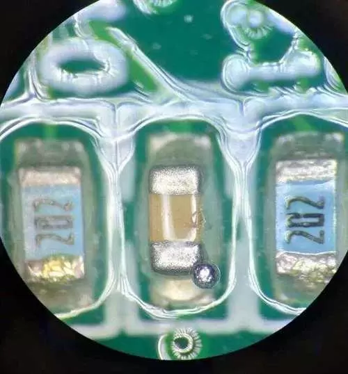
Fine-pitch reality:
● As pad spacing shrinks, mask dams become fragile “slivers.”
● Slivers could lift during reflow, raise risk for solder bridging and shorts.
● Many designers intentionally open mask between ultra-fine pads (or use NSMD pads) based on assembly approaches.
6.3 Positioning Accuracy
Mask positioning is the alignment accuracy between the mask openings and the underlying copper features.
If positioning drifts:
● pads might be partially covered (not fully and poor solder wetting)
● dams can become too thin (sliver lift)
● clearance can shrink (bridging or inspection failures)
Good positioning leads to stable imaging, robust fiducials, and process monitoring.
7. Solder Mask and Via Treatment
7.1 Tented Vias
A tented via is covered by solder mask.
Benefits:
● reduces solder wicking
● improves cosmetic and cleanliness outcomes
● reduces risk of solder balls near vias
Risks:
● poorly formed tents can crack or trap residues
● tenting may fail if via diameter is too large or the mask thickness is insufficient
7.2 Plugged and Filled Vias
● Plugged vias use resin or mask plug to close the hole opening.
● Filled vias (often for via-in-pad) provide a flat surface and stronger solder control.
Non-conductive vs conductive fill:
● Non-conductive is common for preventing wicking and achieving planarity.
● Conductive (copper) filling is higher-performance but more process-demanding.
7.3 When to Leave Vias Exposed
Some vias should stay open:
● test points
● ground stitching vias for EMI strategy (when specified)
● vias designed for heat dissipation or inspection
8. Solder Mask and Surface Finish Compatibility
Solder mask and surface finish don’t “compete”—they have to work together at the pad edges. Most solder mask issues show up where three things meet: mask edge + exposed copper/pad + finishing chemistry/heat. If that interface isn’t stable, you’ll see problems like edge lifting, poor adhesion, or messy pad openings.
ENIG (Electroless Nickel Immersion Gold)
ENIG is generally very mask-friendly for fine-pitch boards because pad planarity is good. The risk is usually not the finish/treatment itself, but mask edge quality:
● Typical issues: thin “mask lips” at pad edges, micro-lifting after reflow, rough pad opening edges if imaging/development is off.
● What helps: tight registration control, clean development to avoid ragged edges, and a solid final cure so the mask doesn’t soften during assembly.
HASL (Lead vs Lead-Free)
HASL introduces more topography (uneven solder thickness), and lead-free HASL typically runs at higher temperatures—both can stress the mask.
● Typical issues: mask thinning on sharp height changes, small cracks near pads, occasional edge pull-back after thermal cycling.
● Optional: choose coating methods that handle uneven surfaces (spray is often more forgiving), maintain proper tack cure to prevent flow, and ensure the cure profile which matches lead-free thermal loads.
OSP (Organic Solderability Preservative)
OSP relies heavily on cleanliness and handling discipline, which also affects mask adhesion near pads.
● Typical issues: contamination at the copper surface leading to weak mask bonding, poor-looking pad edges if prep is inconsistent, sensitivity to rework/extra heat cycles.
● Proper surface prep (clean + controlled micro-etch), strict process cleanliness (no fingerprints/ionic residues), and well-controlled bake/cure so the mask locks in adhesion.
Immersion Silver / Immersion Tin
These finishes can perform well, but they’re more sensitive to storage conditions and process residues, which can indirectly trigger mask-edge problems.
● Typical issues: staining/tarnish concerns near openings, mask-edge discoloration, occasional adhesion complaints if pre-cleaning and post-process rinsing aren’t tight.
● What helps: controlled storage/packaging, disciplined rinsing/drying, and confirming compatibility between the mask system and the finish line chemistry.
Common Adhesion Issues and Practical Solutions
Most “mask vs finish/treatment” problems are actually caused during process. The most common root causes and solutions:
● Poor surface preparation → peeling / edge lifting Solution: strengthen cleaning + micro-etch + activation, reduce time between prep and coating.
● Under-cure or over-cure → soft mask or brittle mask Solution: validate cure profile (time/temperature) for your mask system and lead-free requirements.
● Coating too thick/thin for feature density → slivers or pad encroachment Solution: tune coating method and thickness target; relax dam requirements via DFM for ultra-fine pitch.
● Positioning drift → partial pad coverage or weak dams Solution: improve fiducials and panel stability; align mask expansion rules with fabrication capability.
9. Common Solder Mask Defects and Root Causes
9.1 Misalignment
Symptoms: pad partially covered, uneven dams, shifted openings Causes: poor alignment, unstable imaging, insufficient fiducials, panel dimensional changes Prevention: tighter positioning control, better tooling, DFM review for tight-pitch areas
Symptoms: mask lifts near pads or along traces Causes: weak surface preparation, under-cure, chemical incompatibility, moisture contamination Prevention: robust micro-etch/activation, correct cure profile, moisture control
9.4 Cracking (Common in Flex or Stress Zones)
Symptoms: cracks over areas or near board edges Causes: brittle mask selection, over-cure, mechanical stress, wrong material for flexing Prevention: flex-appropriate materials, design rules for bend zones, controlled cure strategy
9.5 Mask Slivers Lifting During Reflow
Symptoms: thin dams peel and float, creating bridge risk Causes: the width of dams is lower than constraint width, aggressive expansion rules, poor positioning, heavy topography Prevention: DFM-driven dam rules, consider opening mask between pads in ultra-fine pitch, improve alignment control
● Process-driven: preparation, coating, imaging, development, cure control
10. How to Specify Solder Mask Correctly in Your PCB Design Files
10.1 Gerber Solder Mask Layers
You typically provide:
Top solder mask
Bottom solder mask
These layers define where mask is removed (openings) relative to copper pads.
Key point: your CAD mask expansion rules must align with fabrication capability and assembly needs.
10.2 Fabrication Drawing Callouts
At minimum, specify:
solder mask type (e.g., LPI)
color (if required)
any special requirements (high-temp, flex zones, via tenting rules)
acceptance priorities (pad exposure, dam requirements)
10.3 DFM Checklist for Designers
Before release, check:
minimum dam width in tight pitch zones
via-in-pad rules (filled/capped requirements)
high-voltage spacing rules (mask isn’t a substitute for clearance)
test point openings defined clearly
consistent mask expansion strategy
11. Solder Mask Colors: Do They Matter?
Myths vs reality:
Color does not magically change “electrical performance” in normal designs.
What matters is the material system and cure, not pigment.
Where color does matter:
inspection visibility (contrast with silkscreen and copper)
optical applications (LED boards, sensors) where reflectivity and stray light matter
heat absorption differences can matter in niche cases, but it’s rarely the main driver
Choose color based on inspection, branding, and optical needs—not assumptions.
12. IPC Standards for Solder Mask Application
IPC standards matter because they turn “looks OK” into measurable acceptance criteria—especially when you’re building boards that must survive heat, vibration, humidity, and long service life.
IPC-SM-840 (Solder Mask Material Qualification)
IPC-SM-840 is mainly about the solder mask material itself—how the mask system is qualified and what performance it should meet (adhesion, insulation performance, chemical resistance, durability, etc.). In practice, it helps buyers and engineers confirm the mask ink is not just “any epoxy,” but a controlled material system suitable for the intended reliability level.
IPC-6012 (PCB Performance and Acceptance)
IPC-6012 is a broader PCB qualification/acceptance standard. For solder mask, it connects the mask layer to board-level requirements, such as:
● coverage and consistency on the PCB
● acceptable cosmetic vs functional defects
● reliability expectations based on product class
Think of it as: IPC-SM-840 = material standard, while IPC-6012 = finished PCB acceptance standard.
IPC Classes 1 / 2 / 3: What Changes for Solder Mask
IPC product classes reflect the reliability target, and they influence how strictly solder mask issues are judged:
● Class 1 (General electronics): basic functional requirements; cosmetic issues are often tolerated if they don’t affect soldering or insulation.
● Class 2 (Dedicated service / industrial): tighter control; mask alignment, coverage, and defect limits become more important because boards must be more stable over time.
● Class 3 (High reliability): the strictest level; solder mask must be highly consistent because any weakness can become corrosion paths, leakage risk, or assembly defects.
Why This Matters in High-Reliability Industries
In medical, aerospace, automotive, and other high-reliability environments, solder mask is treated as a functional protection layer, not decoration. Standards and class targets help control risks like:
● moisture ingress and corrosion
● leakage or creepage failures at higher voltages
● solder bridging and fine-pitch assembly fallout
● long-term insulation breakdown after thermal cycling
13. Choosing the Right Solder Mask for Your PCB Application
Case guidance:
High-density SMT / fine pitch: LPI or dry film with proven resolution and registration stability
Power electronics: focus on adhesion, thermal stability, and chemical resistance
RF boards: prioritize consistent thickness and stable dielectric behavior; coordinate with impedance strategy
Flex and rigid-flex: choose materials designed for bending; define bend zones clearly in fab notes
14. FAQs: How Is Solder Mask Applied on PCB?
Is solder mask always required?
Not always, but it’s standard for most production boards because it protects copper and improves assembly yield.
Can solder mask affect impedance?
Yes, in high-speed designs solder mask acts as part of the dielectric environment. Consistent thickness and controlled stackup assumptions matter.
Why does solder mask peel after reflow?
Common causes include poor surface prep, insufficient cure, contamination, or too-thin dams that lift under thermal stress.
What is solder mask defined vs non-solder mask defined pad?
NSMD pads are defined by copper geometry; SMD pads are defined by mask opening. Depends on package, pitch, and assembly strategy.
15. Conclusion: Solder Mask Is a Process, Not Just a Layer
Solder mask is one of those fabrication steps that quietly decides whether a project could be assembled smoothly or turns into rework & yield loss. When the process is controlled—surface prep, coating uniformity, UV imaging alignment, development precision, and full cure—you get stable insulation, predictable soldering outcomes, and better long-term corrosion resistance.
If your project includes tight fine-pitch, via-in-pad, HDI features, or might be working in harsh-environment, don’t take solder mask as a default checkbox. Align mask rules with the PCB manufacturing process, confirm manufacturable dams and clearances, and communicate with your manufacturer at early stage for a DFM. That’s how you turn “solder mask on PCB” from “green paint” into a reliability.
As a major of Electronics and Mechanical Automation, Sonic has been engaged in PCB design, R&D, manufacturing of eletronics for around 22 years, as engineering director and coordinates with supply chain(components&CNC parts), providing professional supports and consults for global customers.
This website uses cookies to provide you with a safer and more personal experience. By accepting, you agree to the Cookie Policy and the use of cookies for advertising and analytics purposes.
 en
en


 WhatsApp