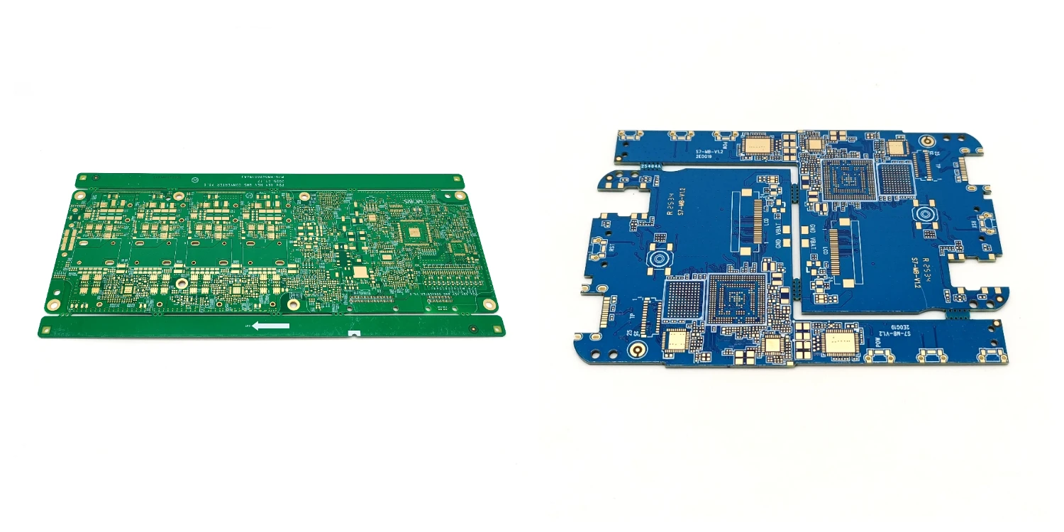
1. What Is PCB Manufacturing?
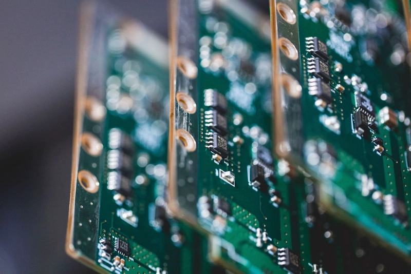
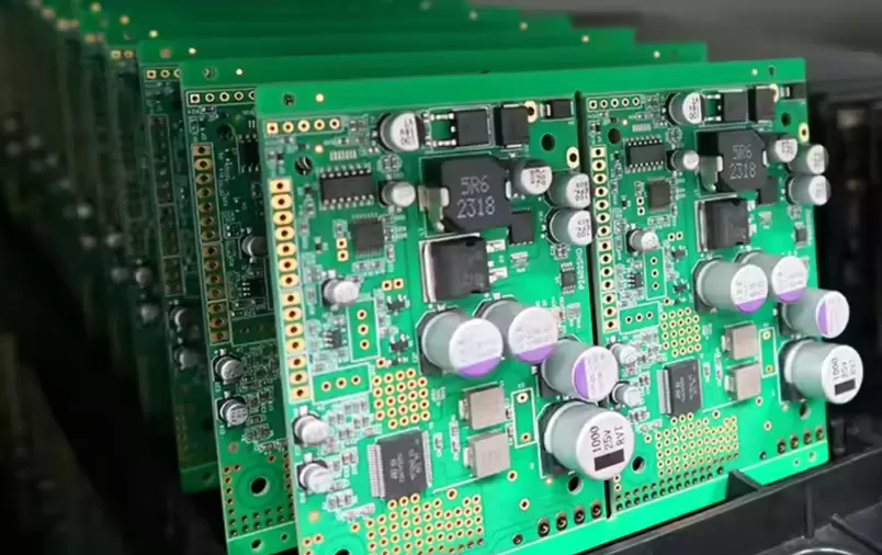
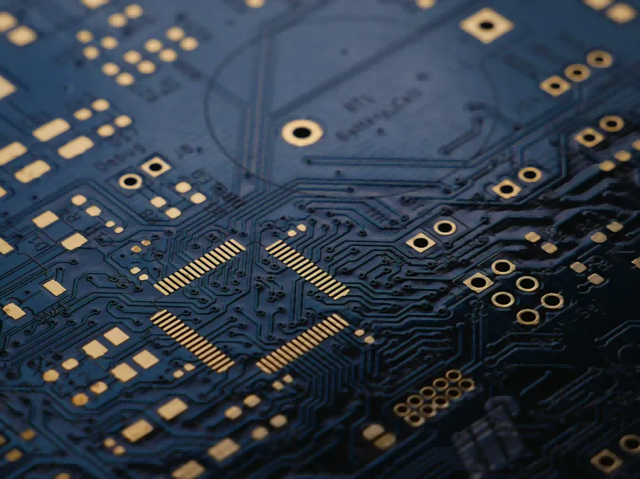
PCB manufacturing (also called PCB fabrication) is the process of turning electronic circuit design files&documents into physical printed circuit board (PCB)—a layered structure made of insulating material and patterned copper that routes signals and power between components.
PCB fabrication vs. PCB assembly (FAB vs. PCBA)
PCB fabrication (FAB) creates the bare board: copper layers, vias, solder mask, silkscreen, and surface finish.
PCB assembly (PCBA) installs components onto the surface of bare board through SMT and through-hole processes, as assembled product.
Why PCB manufacturing quality affects product reliability
Most “mysterious” failures aren’t mysterious at all. They could always be traced back to fabrication progress: marginal plating in vias, unstable impedance, resin voids from lamination, poor solder mask registration, or contamination that shows up later as leakage. A clean, controlled PCB manufacturing process is the basement for everything that follows—signal integrity, thermal performance, assembly yield, and long-term reliability.
2. How a PCB Goes from Concept to Finished Board
Think of PCB manufacturing as a chain and each step “locks” quality for the next one.
Whole-View workflow (design → fabrication → testing)
Design & output files (Gerber, drill, stack-up, notes)
Material prep (laminates, copper, prepreg selection)
Inner layer imaging & etching (for multilayers boards)
Lamination (bonding layers into one panel)
Drilling (through holes, vias, microvias as required)
Hole metallization & copper plating
Outer layer imaging & etching
Solder mask and silkscreen
Surface finish (HASL/ENIG/Immersion Silver/Hard Gold, etc.)
Electrical test and inspection
Profiling / routing / depanelization
Final inspection, packaging, and delivery
Single-layer vs. multilayer workflows
Single-layer: copper patterning happens once, then mask/finish/test.
Multilayer: inner layer always being manufactured first, then laminate with the outer layers. That adds complexity—registration, lamination control, via reliability—also the risk of profile changes.
Where most defects originate
Defects rarely come from one dramatic mistake. They come from small deviations that compound:
Imaging/etching: under/over etch affecting trace width
Lamination: trapped voids, resin starvation, layer shift
Drilling: rough hole walls, misregistration, drill wander
Plating: thin copper in vias, voids, poor adhesion
Solder mask: poor registration causing exposed copper or coverage issues
If you understand where defects originate, it becomes easier to design for manufacturability and choose a supplier who controls the right variables.
3. PCB Design Files That Manufacturers Actually Need
Good fabrication starts with clear and comprehensive files. If your files is not comprehensively integrated, the board might be manufactured “technically correct” but practically unusable.
3.1 Essential files for PCB fabrication
Gerber files
These files define the copper layers, traces&spaces, solder mask, silkscreen, paste layers (if provided), and mechanical outlines. Modern Gerber files include embedded aperture data, reducing ambiguity.
Drill files
Drill files define the locations and diameters of plated and non-plated holes. For complex boards, separate drill files or clear drill tables could avoid misunderstanding.
Stack-up drawings
A stack-up indicates the factory how the board stack up, it should specify:
Layer order
Dielectric thickness
Copper weights (inner/outer)
Material system (FR-4 grade, high-Tg, Rogers, etc.)
Controlled impedance structures (single-ended/differential, target ohms)
Read-me / fabrication notes
This is where critical requirements belong:
Controlled impedance targets and test coupon needs
Finished thickness tolerance
Surface finish preference
Solder mask type
Via structures: blind/buried, via-in-pad, micro-via stacking
Any special requirements (e.g., CAF resistance, cleanliness standards)
3.2 Common design mistakes that delay PCB production
Incomplete stack-ups
“Standard stack-up” sounds convenient, but it’s not universal. Without a defined stack-up, impedance targets and thickness could drift.
Unclear impedance requirements
If you have DDR, PCIe, USB, HDMI, RF traces, or tight timing margins, impedance must be explicit:
target impedance (e.g., 50Ω single-ended, 90/100Ω differential)
tolerance (e.g., ±10%)
reference plane assumptions
coupon requirements for verification
Missing solder mask definitions
Mask openings, expansions, and dam widths, these matter for assembly yield—especially for fine pitch parts. If mask data is incomplete, you may see slivers, bridging risks, or pad exposure issues.
If you want a manufacturer who can help to spot out these potential issues at early stage, Benlida provides PCB engineering support alongside fabrication services through its workflow on Benlida
4. Materials Used in PCB Manufacturing
Materials are where performance starts. Gerber files and use different materials to manufacture, and the boards might behave very differently in real hardware.
4.1 PCB substrate materials
FR-4
FR-4 is a glass-reinforced epoxy which widely applied for electronic products.
High-Tg materials
High-Tg (glass transition temperature) materials help when boards encounter higher thermal stress—multiple reflow cycles, higher operating temperatures, or demanding reliability requirements. They can improve dimensional stability and reduce risk of delamination.
High-frequency (Rogers, PTFE, hybrids)
For RF and high-speed designs, dielectric stability and loss are very important. Materials like Rogers and PTFE-based could systematically reduce loss and improve signal performance, particularly at higher frequencies.
4.2 Copper thickness and it’s impact
Copper Thickness 1OZ vs 2OZ (and beyond)
Copper thickness affects:
current carrying capacity (thicker copper handles more current for the same trace width)
thermal performance (more copper could dissipate heat faster)
manufacturability (thicker copper will make fine traces&space much harder to etch)
A common trade-off: thicker copper boosts power capability but may limit the smallest trace/space that manufacturer can reliably achieve. That’s why it is important to align design intention and manufacturing capability at first beginning.
For multilayer PCB, inner layers are the “foundation.” Errors here if get laminated and buried inside of the board, then it will beyond to fix.
Copper-clad laminate preparation
The laminate is cleaned and prepared to ensure good adhesion of imaging materials and avoid contamination that could affect etching.
Photo-resist application (simple explanation)
Photo-resist is a light-sensitive coating which applied on copper surface, take it like a temporary “protective paint” that determines which copper remains and which copper will be etched away.
UV exposure and circuit pattern transfer
A photo-tool (film) or direct imaging system exposes the photo-resist. Exposed areas are developed, revealing a pattern that matches your design.
Inner-layer copper etching
Etching removes unwanted copper. This is where trace widths and spacing can shift if the process isn’t controlled. In tight designs, small variations can affect impedance or create opens/shorts.
Lamination bonds multiple layers into one rigid structure.
What is prepreg and why it matters
Prepreg is thin fiberglass film pre-impregnated with resin. Under heat and pressure, it melts and cures, becoming the “glue” that bonds layers together while providing insulation between copper layers.
Heat, pressure and epoxy flow
During lamination:
Heat softens the resin
Pressure forces intimate contact between layers
Resin fills gaps and bonds everything
Cooling cures the resin into a stable structure
Common lamination defects and prevention
Voids: trapped air or insufficient resin flow
Delamination: poor bonding due to contamination or incorrect lamination profile
Layer shift: registration problems that cause misalignment
Well-controlled lamination is one of the biggest separators between average and excellent PCB manufacturers.
Drilling is a step that turns a flat laminated panel into a board with interconnections. In the PCB drilling process, every hole is a electrical path—whether it becomes a plated via, a component lead hole, or a mechanical mounting feature. That’s why drilling quality direct impact on reliability, plating performance, and long-term stability.
CNC Mechanical Drilling (for Through Holes)
For most standard designs, CNC mechanical drilling is the most common and cost-effective PCB drilling process. It’s used for:
Through holes for connectors and through-hole components
Standard vias connecting multiple layers
Non-plated holes for tooling and mounting (when specified)
Why tool control matters:
Drill bit, spindle speed, feed rate, and “hit count” (how many holes a bit drills before replacement) all affect the quality of hole wall. Worn tools would create rough hole walls, smear resin, or leave micro-cracks—all of which weaken plating adhesion and reduce via reliability.
Micro-via Drilling Basics (Laser for HDI Density)
When designs require smaller interconnects—especially in HDI—mechanical drilling reaches its limits. Micro-vias are usually made by laser drilling, which allows:
Smaller diameters than standard drills
High-density fan-out for BGAs and compact modules
Shorter interconnect paths for better electrical performance
In practice, laser-drilled micro-vias support tight routing and layer-to-layer connections without consuming as much board as traditional vias.
Why Hole Accuracy Determines Via Reliability
At the end, PCB via holes are only reliable if the drilled geometry is clean, consistent, and correctly placed. A via is only as good as the hole, it starts with:
Smooth hole walls support strong copper adhesion during metallization and plating
Accurate hole diameter helps achieve consistent plating thickness and stable resistance
Correct registration ensures PCB via holes land cleanly on pads, maintaining annular ring integrity and reducing breakout risk
Clean drilling reduces resin smear, improving inner-layer connectivity and long-term durability
If your design includes dense via fields, tight tolerances, or HDI structures, drilling quality is most important and requires process management rigorously.
8. Through-Hole Metallization and Copper Plating
After drilling, holes are just empty cylinders through insulating material. To connect layers electrically, those holes must be plated.
Why drilled holes must be plated
Plated holes create conductive pathways between copper layers—essential for multi-layer connections and through-hole components.
Chemical copper deposition
A thin initial copper layer is deposited chemically so that the hole walls become conductive.
Electrical interconnection between layers
Once conductive, the board goes through electrolytic plating to build copper thickness in holes and on surfaces.
Plating thickness control
Thickness control matters for:
via reliability (too thin will increase crack risk)
current carrying capacity
long-term durability under thermal cycling
9. Outer Layer Imaging and Final Circuit Formation
Outer layers are built after lamination, drilling, and initial plating.
Outer-layer photo-resist process
Like inner layers, outer layers use photo-resist, exposure, and development to define copper patterns.
Differences vs. inner layers
Outer layers must consider:
existing plated copper thickness
via pads and annular ring requirements
final trace width after plating and etching
Final copper etching principles
After pattern plating (depending on process), unwanted copper is etched away to reveal final outer circuits.
10. Protective and Functional PCB Coatings
Solder mask protects copper from oxidation and prevents solder bridging during assembly. It also improves insulation and reduces accidental shorts.
Common solder mask colors exist for practical reasons (contrast, inspection preference, branding), but color alone is not a performance guarantee. What matters is mask quality, registration, adhesion, and thickness control.
Silkscreen adds:
Designators reference
polarity marks
assembly and inspection guidance
traceability information (lot codes, identifiers)
In real production, clean silkscreen could reduces mistakes during assembly and speeds up inspection.
Surface finish protects copper pads and ensures good solderability. The “best” finish depends on component types, shelf life, and performance requirements.
Finish | Cost | Shelf Life | Lead-Free | Best Use Case |
HASL | Low | Long | Optional | Cost-sensitive designs |
ENIG | Medium | Long | Yes | Fine-pitch components |
Immersion Silver | Medium | Short | Yes | High-frequency boards |
Hard Gold | High | Very Long | Yes | Edge connectors |
A practical way to choose: start from your assembly requirement (fine pitch, BGA, connector wear, RF loss) and work backward to the finish that supports it with minimal risk.
Testing verifies that what you designed is what you received.
Continuity and isolation testing
Continuity checks that nets connect where they should
Isolation checks that nets don’t short where they shouldn’t
Flying probe vs fixture testing
Flying probe: flexible, good for prototypes and lower volumes
Fixture testing: fast for volume production but requires a test fixture
Why testing is non-negotiable
Skip the testing process could save time today but it leaves risks in future: if any short or open shows up after assembly, the costs of components and assembly labor, debug time, and schedule, all will be wasted away. Electrical testing is one of the most important process for reliability.
13. PCB Profiling, Routing, and Board Separation
After fabrication and finishing, the board must be shaped by following design requirements.
CNC routing
Routing by CNC, to cut the final outline.
V-scoring
V-scoring creates a controlled “V-cut” so boards could be separated cleanly from there, after assembly — commonly in panelized production.
Choosing the right depanelization method
Use routing for complex shapes or when edge quality matters
Use V-scoring for straight-line separation and high throughput
Consider assembly stresses: poor depanelization choices can crack solder joints or damage components
14. Final Inspection, Packaging, and Delivery
Visual inspection
Inspection for visible defects: solder mask issues, scratches, missing markings, surface finish anomalies.
Dimensional accuracy
Verifies board outline, hole-to-hole distances, and critical features—especially important for connector alignment and enclosures.
Vacuum packaging and moisture control
Proper packaging could reduce oxidation and moisture absorption. For sensitive materials, moisture control could avoid issues during reflow.
15. How to Choose the Right PCB Manufacturer
This is the knowledge of process becomes a real purchasing advantage. The “right” partner isn’t just the one with the lowest price—it’s the PCB manufacturer who can consistently achieve your technical targets, your schedule, support you with engineering capacity and from prototype to mass production.
Capability checklist
When evaluating a PCB supplier, don’t just ask “Can you make it?”, ask “Can you make it repeatably?” Confirm they can reliably support:
Layers and stack-up requirements: Can they build your exact stack-up and achieve thickness targets?
Trace/space and drill tolerances: Especially important for dense routing and fine-pitch components.
Controlled impedance verification: Ask how impedance is built, measured, and reported (coupons, test methods, tolerances).
Special materials: High-Tg FR-4, Rogers/PTFE, and hybrid constructions for RF/high-speed designs.
HDI features: Micro-vias, blind/buried vias, via-in-pad (and whether VIPPO is supported when needed).
Surface finish options: ENIG/ENEPIG/Immersion Silver/HASL/Hard Gold—matched to your assembly and reliability goals.
If your product has tight electrical margins, choose a partner whom has proved custom PCB fabrication capability—because process control matters more than marketing claims.
Quality certifications and process proof
Certifications can be a useful baseline, but what really separates a dependable PCB manufacturer is how they control quality day-to-day. Check for:
IQC/Incoming material inspection (laminates, prepreg, copper, chemicals)
Process control points throughout imaging, etching, drilling, lamination, and plating
Cross-sectioning and plating verification (via wall copper, annular ring, resin fill where applicable)
Electrical testing coverage (flying probe vs testing fixture, continuity/isolation strategy)
Traceability and lot control (issues can be isolated and prevented from repeating)
A strong PCB supplier will be able to explain these controls clearly and show typical inspection/testing outputs, not just promise them.
Turnaround time vs cost trade-offs
Fast quotes don’t always mean fast boards, and low unit pricing doesn’t always mean low total cost. The best partners help you to balance:
Yield (first-pass success rate)
Rework risk (hidden cost of marginal builds)
Schedule stability (realistic lead times and predictable delivery)
Technical support (DFM feedback, engineering communication)
Long-term consistency (repeatability across batches)
In practice, the best value often comes from a PCB manufacturer who prevents problems at early stage—especially for advanced designs where custom PCB fabrication quality directly affects assembly yield and field reliability.
If you’re looking for a PCB manufacturer, comparing PCB supplier capabilities, or planning custom PCB fabrication for a new project, Benlida provides PCB fabrication and engineering support through all the process, you can know Benlida more from website here.
16. Frequently Asked Questions About PCB Manufacturing
How long does PCB fabrication take?
Lead time depends on layer count, materials, special processes (HDI, controlled impedance), surface finish, and testing requirements. Prototypes can be faster, while complex multilayer boards may require more process steps.
What affects PCB manufacturing cost?
The biggest cost drivers typically include:
layer count and board size
material selection (standard FR-4 vs high-frequency laminates)
fine features (tight trace/space, small drills)
special via structures (blind/buried, microvia stacking)
surface finish choice
testing and inspection requirements
What tolerances are realistic?
Realistic tolerances depend on design complexity and materials. The best approach is to align tolerances with functional needs—then confirm manufacturability with your chosen supplier before production starts.
Can prototypes and mass production use the same process?
The core steps are similar, but tooling, panelization, test strategy, and process optimization may differ. A strong manufacturer can build prototypes that scale cleanly to mass production without redesign surprises.
17. Conclusion: Why Process Knowledge Leads to Better PCBs
PCB manufacturing isn’t magic—it’s a chain of controlled steps where each stage affects the next. When designers understand the process, they make better decisions about stack-ups, materials, vias, and tolerances. When manufacturers run disciplined processes, boards deliver consistent electrical performance, assembly yield, and long-term reliability.
If you’re planning a new board or troubleshooting manufacturing yield, collaborating early with a capable fabrication partner, that would make the difference. To explore fabrication capabilities, engineering support, and manufacturing services, visit Benlida.
Related PCB manufacturing processes
PCB Inner Layer Imaging & Etching Process
What is the PCB Lamination Process?
How do drilling (mechanical/laser) processes work in PCB manufacturing?
What is the plating process in PCB Manufacturing?
How are vias formed in PCBs?
How is solder mask applied on PCB?
Ultimate Guide to PCB silk screen printing process
What is the surface finish process in PCB?
What are the most common methods of PCB testing?
About the auther:

Sonic Yang
As a major of Electronics and Mechanical Automation, Sonic has been engaged in PCB design, R&D, manufacturing of eletronics for around 22 years, as engineering director and coordinates with supply chain(components&CNC parts), providing professional supports and consults for global customers.
 en
en


 WhatsApp