In electroplating process, current density is not only a core parameter but also determines the quality and reliability of the plating layer. Controlling the deposition behavior of metal ions on the cathode surface, it determines the crystal morphology, physical properties, and long-term stability of the plating layer.
I. Why is Appropriate Current Density Crucial?
When the current density is within the optimal range, the electrochemical deposition process reaches dynamic equilibrium:
● Nucleation and Growth Coordination: The rate at which metal ions are reduced to atoms (nucleation rate) matches the grain growth rate. At this point, a large number of crystal nuclei are generated uniformly, while growth is inhibited, resulting in a fine, dense, and bright plating layer.
● Optimal Performance: This structure means that the plating layer has higher hardness, better corrosion-resistance, lower porosity, and excellent conductivity and solderability.
II. Failures Caused by Inaccurate Current Density
Once the current density deviates from the optimal range, various defects will follow as:
1. Low Current Density – Roughness and Porosity
● Phenomenon: The plating layer is dull, rough, spongy, or powdery, with poor adhesion.
● Mechanism: The nucleation rate is much lower than the growth rate, allowing only a few nuclei to grow sufficiently, forming coarse grains. Additives in the plating bath (such as brighteners and leveling agents) also cannot function effectively due to insufficient polarization.
2. Excessive Current Density – Scorching and Brittleness
● Concentration Polarization: Metal ions on the cathode surface are rapidly consumed, and replenishment is insufficient, leading to a large amount of hydrogen evolution, which mixes in the coating, forming a loose, brittle "scorched" layer.
● Internal Stress: Excessively fast deposition rates prevent atoms from arranging themselves in an orderly manner, generating extremely high internal stress, causing the coating to become brittle and peel.
● Phenomenon: Dark, rough, charred deposits appear at the edges or protrusions of the coating, indicating a sharp increase in internal stress, making it extremely prone to cracking and peeling.
3. Other Issues
● Poor and Uneven Plating: Different thickness between high and low current zones, but deep holes have no coating.
● Abnormal Additive Consumption: Additives decompose and become ineffective in high-current zones, while they accumulate and become overdeposited on low-current zones.
● Anodic passivation: Imbalance in the matched anodic current density leads to anodic passivation and decrease the concentration the main fluid.
III. Other Factors Leading to Electroplating Failure
A high-quality plating layer is the result of precise and coordinated control of multiple factors. Uncontrolled current density is the core factor leading to electroplating failure, but there are other factors as well:
1. Pretreatment: Degreasing and pickling unthroughly, poor activation, resulting in poor adhesion, blistering, and peeling.
2. Process parameters: Improper current density, temperature, pH, and stirring, directly determine the crystal morphology and physical properties.
3. Plating materials: Imbalanced composition, impurity, contamination, and additive imbalance, directly affect the deposition reaction and crystallization process.
4. Post-treatment: Inadequate cleaning and improper passivation, lead to pitting, corrosion, discoloration, and poor solderability.
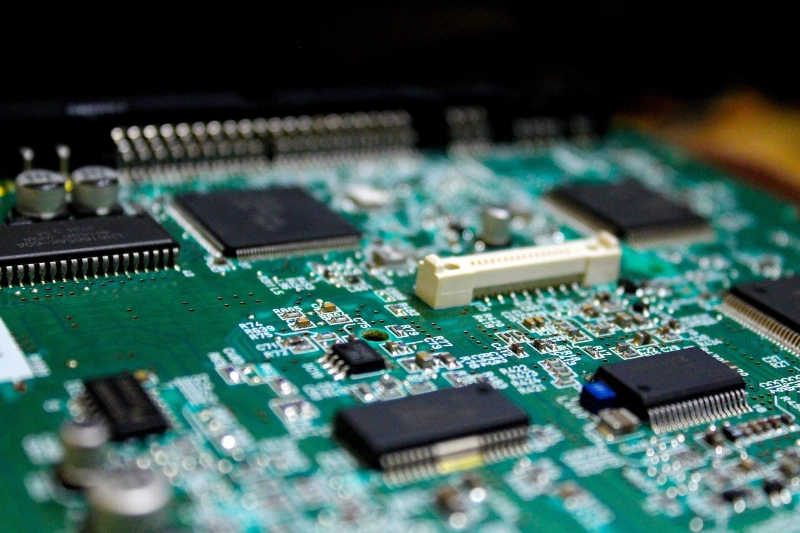
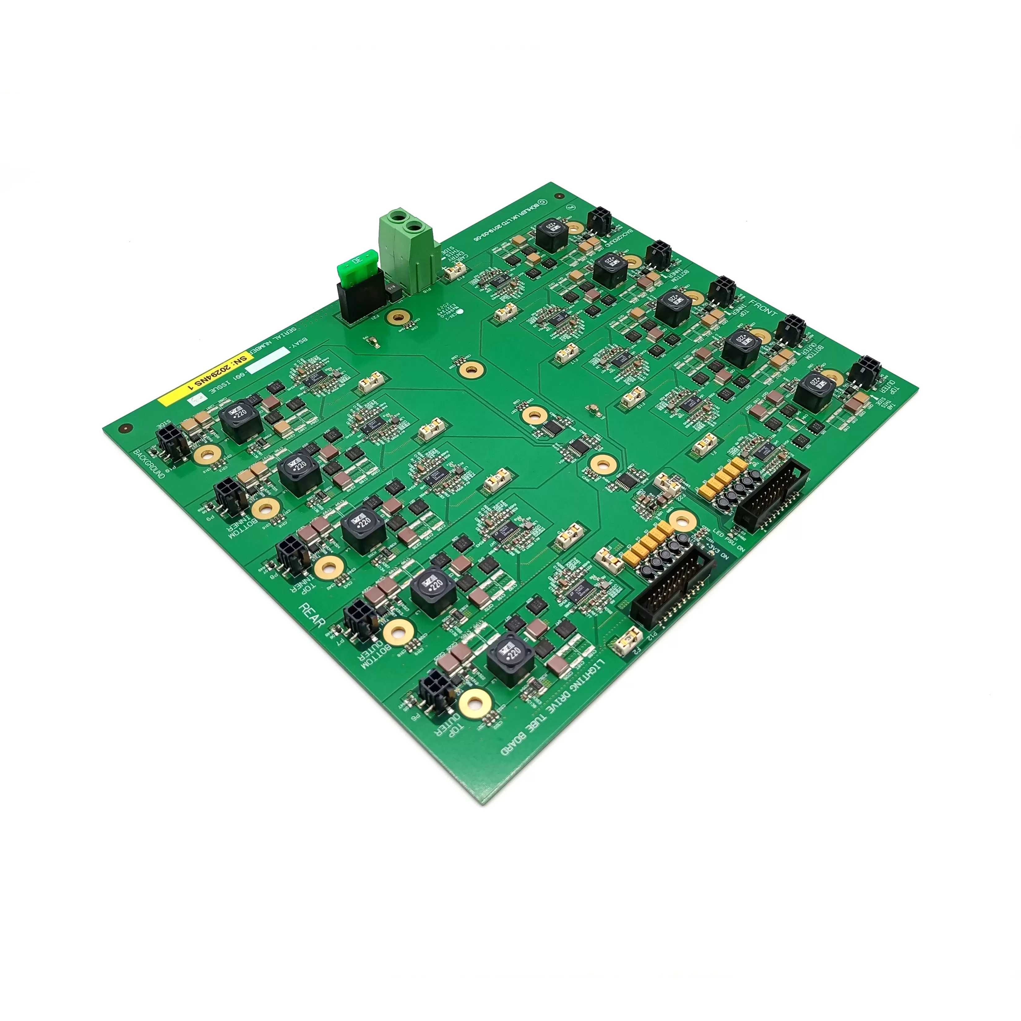
Benlida has been manufacturing PCB for 14 years, relying on professional equipments and engineering&quality team, we monitor the production process strictly, from macroscopic performance to microscopic structure, ensure the quality of electroplating: Is the current density accurate and optimal? Is the plating layer internally good? Are there any risks of failure?
Precise Quantification for Coating Performance
1. Thickness and Composition: X-ray fluorescence spectroscopy (XRF) and coulometric methods are applied to measure the coating thickness and alloy composition accurately.
2. Porosity Testing: The density of the coating is assessed by nitric acid vapor and electrochemical imaging methods, to assess its protective capability.
Analysis for Microstructure
1. Crystallization Observation: High-resolution scanning electron microscopy (SEM) is applied to observe the grain size, density of the crystals on the coating surface, cross-section, to determine the suitability of the current density.
2. Analysis for Composition and Interface: Energy dispersive spectroscopy (EDS) is applied to analyze the elemental distribution of the coating and eliminate impurities; combined with focused ion beam (FIB) to prepare cross-sections, the interfacial bonding state between the coating and the substrate is precisely analyzed.
Verification for Comprehensive Reliability
1. Adhesion Testing: Bending, cross-cut adhesion, and thermal shock tests are conducted to evaluate the coating adhesion.
2. Corrosion Resistance Testing: Neutral salt spray, CASS acetate mist, and sulfur dioxide tests are performed to verify the protective performance of the coating.
3. Solderability Testing: Evaluates the solderability of plating layers (e.g., gold plating, tin plating).
Process Diagnosis and Comprehensive Analysis:
Combining test data, we reverse-engineer the plating solution composition and process parameters to provide a scientific basis for production line adjustments.
When you encounter issues such as:
- Appearance defects: such as rough, blackened, and burnt-like plating
- Adhesion defects: such as blistering, cracking, and peeling
- Other failures: such as rust, poor soldering
- Quality verification: when develop new approaches
Welcome to contact Benlida for consults and learn more about production processes. We are a professional PCB manufacturer and looking forward to manufacture PCB and PCBA for you!
 en
en

 WhatsApp