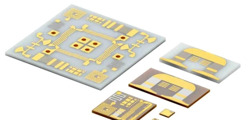
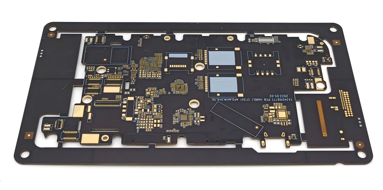
PCB layout and routing is a core process of hardware design, placing components and drawing conductive traces on PCB, directly impacting circuit performance, reliability, and EMC. The following are key principles, considerations and techniques for PCB design, divide into two parts: layout and routing:
I. Layout Principles and Techniques
1. Zoning Planning
● Zoning by functional modules: such as power supply, analog, digital, RF, etc., to avoid mutual interference.
● Signal flow planning: Layout according to the "input → processing → output" flow to reduce crosstalk.
● Sensitive circuit isolation: Keep high-frequency, clock, reset, and other signals away from interference sources.
2. Prioritizing Critical&Functional Groups of Component
● Fixed-position components first: such as connectors, switches, indicator lights, etc.
● Centering core components: such as MCUs, FPGAs, etc., placing related circuits around them.
● Heat-generating components: Consider heat dissipation: Reserve space for heat dissipation, placing them near edges or heat sinks.
3. Layout for Power Supply
● Compact layout: Place DC-DC converters, LDOs, etc., as close to the load as possible to reduce loop area.
● Filter Capacitor Placement: Place large capacitors (e.g., electrolytic capacitors) far away, and small capacitors (e.g., ceramic capacitors) close to the chip's power supply pins.
4. Layout for Decoupling Capacitor
● Place them as close as possible to the chip's power supply pins (on the same layer), and connect vias directly to the power/ground plane.
● Use multiple small capacitors in parallel (e.g., 0.1μF + 0.01μF) to cover a wider frequency band.
5. High-Frequency and Clock Circuits
● Place the clock chip close to the target device and shorten the traces.
● Place the crystal/oscillator close to the IC, prohibit traces underneath it, and use ground shielding.

II. Routing Principles and Techniques
1. Trace Width and Current
● Power Line Width Calculation: Calculate the width appropriately based on the current (e.g., 1A/mm width), leaving a margin.
● Signal Line Width: Typically 4-8mil; impedance control lines are calculated based on the stack-up.
2. Trace Angle
● Avoid sharp angles (<90°), prioritize 45° angles or rounded traces to reduce impedance abrupt changes.
3. Differential Pair Routing
● Use equal-length, equidistant, parallel traces, with length differences typically kept within 5 mils.
● Avoid crossing split reference planes to maintain impedance consistency.
4. Signal Integrity
● Critical signals (e.g., clock, high-speed data) should be short and straight, minimizing vias.
● Adjacent layer traces should be orthogonal to reduce crosstalk.
● 3W Rule: Spacing ≥ 3 times trace width to reduce coupling.
5. Ground Plane and Return Path
● Maintain a complete ground plane and avoid signal lines crossing split ground planes.
● Provide a continuous ground reference layer below high-speed signals, to ensure the shortest return path.
6. Via Usage
● Use multiple power vias in parallel to reduce impedance.
● Reduce the number of vias for high-speed signals (typically ≤ 2).
● Avoid vias on pads (except for BGAs); via-in-pads require fill treatment.
7. Power Tree Routing
● Routing like tree topology to avoid common impedance interference.
● Single-point connection for analog/digital ground (usually using a 0Ω resistor or ferrite bead).
III. EMC/EMI Design Considerations
● Shielding and Filtering: Use shielding covers or ground vias to isolate RF, clock, etc.
● Board Edge Treatment: Keep sensitive signals away from board edges to prevent radiation.
● Grounding Strategy: Use a complete ground plane for multilayer boards and properly segment mixed signal grounds.
IV. Checklist (After Layout and Routing)
● DRC Check: Trace width, spacing, via diameter, etc., meet process requirements.
● Connectivity Check: No unconnected networks.
● Power Integrity: Low impedance power paths, voltage drop meets requirements.
● Signal Integrity: Continuous impedance for high-speed signals, no significant reflections or crosstalk.
● Thermal Design: Unobstructed heat dissipation paths for heat-generating components.
● DFM: Component spacing meets soldering requirements, mark points, process edges, etc. are complete.
V. Advanced Techniques
● Use Ground Vias: Place ground vias near signal layer transitions to provide a return path.
● Blind/Buried Vias and HDI Technology: High-density boards can reduce the number of layers and improve performance.
● Simulation Assistance: Perform SI/PI simulations on critical signals to optimize routing parameters.
Summary:
PCB layout and routing require a balance between electrical performance, manufacturing costs, and design complexity. In practice, the order of "layout first, then routing; critical signals first, then general signals" should be followed, and adjustments should be made flexibly based on the specific circuit characteristics. For high-speed, high-frequency, or high-precision circuits, it is recommended to refer to the chip manufacturer's design guidelines and perform simulation verification.
If you need PCBs and PCBAs, please feel free to contact Benlida! Benlida is a professional PCB&PCBA manufacturer, providing EMS(Electronics Manufacturing Service) for 14 years, with advanced equipment and experienced engineering team, Benlida is committed to providing excellent service to global customers!
About the auther:

Sonic Yang
As a major of Electronics and Mechanical Automation, Sonic has been engaged in PCB design, R&D, manufacturing of eletronics for around 22 years, as engineering director and coordinates with supply chain(components&CNC parts), providing professional supports and consults for global customers.
 en
en


 WhatsApp