The solder mask is the "armor" of PCB which ensures the long-term stability. Its core functions include: prevent short circuits from solder, electrical insulation, and protection from chemical&corrosion. These functions are based on the fundamental premise of a strong adhension between solder mask and substrate. When this protective layer "blisters" or even peels off after gone through the high-temperature wave soldering, it not only signifies failure of protection but also might trigger short circuits, corrosion, even systemic malfunctions and failure. This article is going to analyze the root causes of solder mask blistering and share systematic solutions.

I. The Essence of the Phenomenon: Solder Mask Blistering is the exposure of interface failure
Solder mask blistering is essentially the breakdown of the bonding between the solder mask and the substrate (or copper surface) at high temperatures. The gas or vapor pressure pushes up the solder mask layer, forming the visible "bubbles." Solder intrusion indicates that the interface has completely cracked, creates capillary channels for melt solder.
II. Root Cause: Blistering is the result of a synergistic failure of materials, processes, and design.
1. Materials: Substrate and Solder Mask Ink
● Substrate Contamination: Dust, grease, and residues which remained after drilling, grinding, and cleaning are fatal to interfacial bonding. The most common issue, "insufficient micro-etching," leads to insufficient roughness of the copper surface, preventing bonding and mechanical adhesion.
● Issues relate to Solder Mask Ink
Improper Cleaning: pre-treatment before solder mask application (such as mechanical brushing or chemical cleaning) failed to remove the residual contaminants.
● Ink Properties: The glass transition temperature (Tg) of the ink resin is too low, or the coefficient of thermal expansion is severely mismatched with the substrate. At peak temperatures (often above 260℃) during wave soldering, it's strength drops sharply, or the difference in coefficients of thermal expansion is too large.
● Poor Ink Curing: Insufficient pre-baking or curing, leave solvent residue which violently vaporizes during following processes with high-temperature.
2. Processes: Accumulation of Defects in the Manufacturing Process
● Uncontrolled Solder Mask Printing and Curing Process: Inadequate energy for exposure, developing parameters, curing temperature, and time in short, any of these factors might lead to insufficient viscosity and poor adhesion.
● Surface Treatment Process: some surface treatment approaches, such as OSP or silver immersion, if contaminate the solder mask interface, will reduce adhesion significantly.
● Thermal Impact during Wave Soldering: Uneven preheating, excessively high peak temperatures, and excessively long period for high-temperature, all could cause fatal impacts on the interface bonding.
3. Design Dimension: Ineffective Dissipation of Thermal Stress
Uneven Distribution of Copper Foil: differences in heat capacity and expansion rate between large copper areas (such as the power layer) and substrate areas which covered only by solder mask, they create substantial stress at the interface, leading to blistering.
III. Solutions: From Prevention to Control
1. Incoming Material Inspection and Process Control
● Inspection for Interface Cleanliness: Inspect micro-etching and cleanliness before solder mask pretreatment, to ensure optimal activation on the copper surface.
● Verification for Ink: Follow the supplier's recommended curing profile strictly and conduct adhesion tests (e.g., cross-cut adhesion test).
● Isolation for Surface Treatment: Ensure a clear boundary between the solder mask opening area and the surface treatment area, to avoid chemical contamination.
2. Optimize Process of Wave Soldering
"Gentle and soft" Wave Soldering Profile: While ensuring adequate solder application, lower the peak temperature and shorten the time, to reduce thermal shock.
Preheating: heating the PCB and solder mask layer, slowly&gently, to reduce the violent inflation from internal vapor.
3. Design Collaboration
Solder Mask Opening Design: Consider to apply solder mask bridges or mesh openings at the edges of large copper areas, to buffer thermal stress.
Solder Mask Blistering: A Red Flag for PCB Reliability
Solder mask blistering after wave soldering is not only a defect on surface, it signifies fundamental defects, such as interface contamination, poor curing, poor thermal matching within the PCB. Like blisters, if not eradicated such defects completely from manufacturing process, it will increase the quality risks and hurt reliability of the electronic products. Rigorous inspection for materials, monitor the processes, and optimize the design, are 3 cores to prevent such defects and ensure the reliability of PCB.
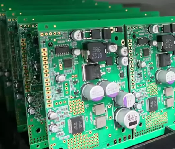
Benlida has been manufacturing PCBs for 14 years, providing reliable products and high-quality services to customers, from domestic to global markets. If your products encounter solder mask blistering issues, please contact Benlida for analysis services and to learn about Benlida's quality control and product quality.
Benlida is ready to serve you!
 en
en

 WhatsApp