Resin-plugged and solder masking are very common&important processes on vias in PCB (Printed Circuit Board) manufacturing. They are two different methods for vias treating on PCBs, with significant differences on purpose, process, and application scenarios.
This article will provide a detailed comparison and explanation from multiple perspectives.
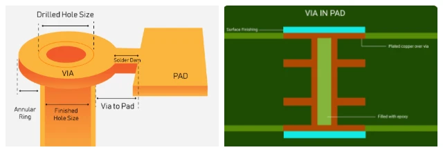
Core Concepts:
● Resin-Plugged Vias: Primary aim is to prevent solder paste from flowing out of the vias during soldering, which might cause short circuits, cold solder joints, or recessed pads at the via opening. It is a functional, internal filling process. Typically used for vias in BGA (Ball Grid Array) package areas.
● Solder Masking Vias: Primary aim is to prevent flux and other contaminants from remaining in the via and to maintain a flat board surface for easy mounting. It is a surface treatment and solder mask process. Typically used for screw holes, positioning holes, or ordinary vias in non-wiring areas.
Detailed Comparison:
Characteristics: Resin-Plugged Vias Solder Masking Vias
| Comparison | Resin Plugging | Solder Masking |
| Core Purpose | Prevents solder short circuits and avoids solder balls, flowing to the back side of the BGA area through the via. | Ensure electrical reliability. Maintain a flat board surface to prevent contaminant and meet customer's requirements for appearance and cleanliness. |
| Process Location | Typically performed after inner layer circuitry fabrication and before lamination, or after lamination and before outer layer circuitry fabrication. This is a mid-stage process in PCB manufacturing. | Perform after outer layer circuitry etching and before surface treatments (such as tin plating or immersion gold). This is a final stage in PCB manufacturing. |
| Materials | Specialized epoxy resin with good flowability, low shrinkage after curing, and high thermal stability. | Ordinary solder mask ink, also known as "green oil," is the same material as the solder mask on the board. |
| Process Flow | 1. Drilling
2. Resin plugging (printing or vacuum filling)
3. Baking and curing
4. Grinding and polishing (removing excess resin to smooth the surface)
5. Continue with subsequent lamination/circuit fabrication | 1. Complete all circuitry and drilling
2. Print solder mask ink (covering both vias and surface simultaneously)
3. Pre-baking
4. Exposure and development (exposing the pads to be soldered)
5. Final curing |
| Surface Condition | After plugging and grinding, the surface is absolutely smooth and can be completely flush with the copper surface, facilitating subsequent pad fabrication. | The surface has slight dents (the ink shrinks during curing), appearing concave. Pads cannot be placed on this surface. |
| Electrical Impact | After filling, the holes are no longer conductive (unless specifically designed with conductive resin). | The conductivity of the vias remain unchanged; the vias inner-walls are still copper-plated, maintaining conductivity. |
| Cost | Very high. Due to the addition of two complex processes, resin filling and grinding, the process requirements are extremely high. | Very low. This is simply an indirect step in the standard solder mask process, incurring almost no additional cost. |
| Key Application Scenarios | 1. Vias under BGAs (crucial)
2. Vias requiring pad-to-pad via design
3. High-density interconnect boards, preventing short circuits
4. Products requiring high reliability: | 1. Non-metallic screw holes/locating holes
2. Ordinary through-holes where customers explicitly require protection from contaminants
3. Products with stringent requirements for board cleanliness |
How to Choose?
1. Location and function:
● If the via is on or very close to a BGA pad, resin plugging is mandatory; otherwise, a short circuit might occur during SMT soldering.
● If the via is in a non-routing area and is only for aesthetics or contamination prevention, solder mask plugging is sufficient.
2. Design requirements:
● If the design involves pad-to-pad vias (i.e., the via is centered on the pad), resin plugging and grinding are necessary to allow for pad placement and soldering.
● If it's just a simple through-hole, no soldering is needed, and solder masking is optional (depending on the PCB manufacturer's standards).
3. Cost budgets:
● Resin plugging increases PCB manufacturing costs significantly and lead times. It should be avoided unless absolutely necessary.
Common Misconceptions:
Misconception 1: Can solder mask prevent BGA short circuits?
● No! Solder masking is a thin layer inside the hole, and its surface is recessed. During high-temperature soldering, molten solder paste can easily break through this layer and flow into the hole, leading to insufficient solder joints or short circuits due to solder penetration on the back side.
Misconception 2: Can resin-plugged vias still conduct electricity?
● After standard resin plugging, the via is filled with insulating resin, and there is no longer any electrical conductivity between the upper and lower layers through this hole. If this hole is used for interlayer conduction, it is essential to ensure that the via walls are properly metallized before plugging, and that the resin only fills the via without damaging the copper plating. Sometimes a "cap-via" design is used, where only the two ends of the via are sealed with resin, leaving the middle hollow and conductive. However, this process is more complex.
Misconception 3: Can you identify them directly by appearance?
On the finished board, observation could identify them:
● Resin-plugged vias: The via opening is flat and the resin material may be visible (the color may differ from the solder mask, or it may appear copper-colored if copper plating was done after grinding).
● Solder masking vias: There is a distinct circular indentation in the center of the via opening, and the color matches the surrounding solder mask.
Summary:
● Resin-plugged vias: Functional filling, solving electrical reliability issues (short circuit prevention), high cost, complex process.
● Solder masking vias: Surface solder mask, solving appearance and cleaning issues, low cost, simple and convenient.
When design a PCB, it is necessary to communicate with the PCB manufacturer, regarding the location and function of the vias, clearly specifying the via plugging or masking requirements, to ensure reliability of PCB and cost control. In the BGA area, resin plugging is usually a mandatory process requirement.
Benlida focuses on PCB manufacturing and assembly for 14 years, we have been providing excellent PCB&PCBA, so as other service to customers. If you and your PCB are having demands for via filling technique, please contact Benlida and let's discuss more!
 en
en


 WhatsApp