Component mounting on FPCs (Flexible Printed Circuit Boards) (usually referring to SMT surface mount technology) is a highly challenging and precise process. It's core difficulties come from the flexibility, susceptibility to deformation, low heat resistance, and unevenness of FPC substrate. The following will systematically explain it's process flow, key process points, and precautions.
I. Core Process Flow of FPC SMT Assembly
A complete FPC SMT process requires specialized fixture/carriers and meticulous process control.
1. Preliminary Preparation: FPC Fixing and Carrier Design
● Using a Carrier (Jig/Pattern)
This is a prerequisite for successful FPC SMT. Carriers are typically made of high-temperature resistant synthetic material or aluminum-magnesium alloy, with grooves engraved to match the FPC's shape for positioning and physical support.
● Fixing Methods:
* High-Temperature Tape: Adhering the FPC to the carrier around it's edges is the most common approach. Specialized tape with high temperature resistance and minimal residue should be selected.
* Magnetic clamping/cover plate: For FPCs with dense components or requiring double-sided mounting, metal carriers with magnetic covers provide uniform flatness pressure.
* Vacuum adsorption: High-end carriers are designed with vacuum holes, using negative pressure to flatten and adsorb the FPC onto the fixture.
2. Solder paste printing
● Use a semi-automatic or fully automatic printer.
● Critical: Due to the grooves on the carrier, the printer platform must be absolutely level to ensure uniform squeegee pressure.
● Stencil: Laser-cut stainless steel stencils are typically used, sometimes with localized compensation designs to accommodate minor deformations of the FPC.
● Solder paste selection: It is recommended to use fine-particle solder paste of grade 4 (25-38μm particle size) or grade 5 (15-25μm), which has good flowability and is suitable for small pads on FPCs.
3. Component placement
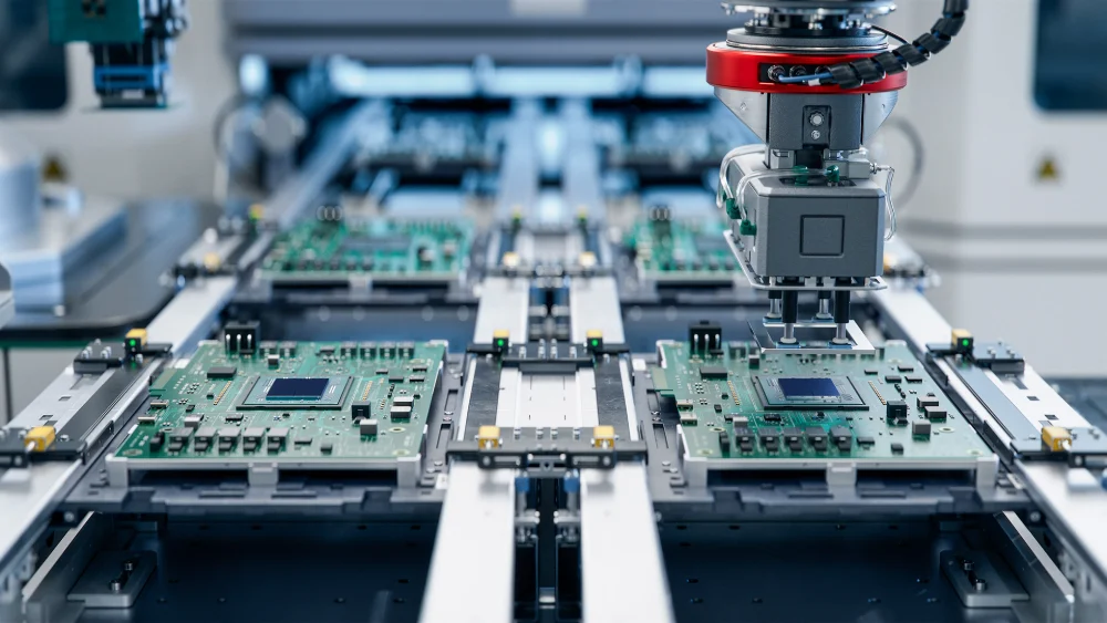
● Use a high-precision pick-and-place machine.
● Similar to rigid PCB assembly processes, but the following points should be noted:
* Choose the appropriate nozzle to avoid localized deformation or damage to the FPC due to excessive pressure.
* The mounting height (Z-axis) needs to be precisely set, taking into account the total thickness of the FPC and carrier.
4. Reflow Soldering
● This is the most critical step. The temperature resistance and heat capacity of the FPC differ from those of rigid PCBs.
● Reflow Temperature Profile: A gentle profile of "low temperature, slow baking" must be used.
* Preheating Zone: The heating rate should be slow (usually 1-2°C/s) to allow the FPC and carrier to be heated evenly and avoid thermal stress.
* Isothermal/Activation Zone: The time should be appropriately extended to ensure sufficient flux activation and evaporation of moisture inside the FPC.
* Reflow Zone: The peak temperature should be about 5-10°C lower than the recommended solder paste value, usually controlled between 230-245°C. The duration (TAL) should be short to reduce thermal shock.
● Carrier Function: In the reflow oven, the carrier not only provides support but also helps to evenly dissipate heat and prevent localized overheating.
5. Cooling, Inspection, and Post-Processing
● Cooling: Natural cooling or controlled cooling rate is used to avoid rapid cooling that can cause solder joint brittleness or FPC deformation.
● Inspection: Use AOI (Automated Optical Inspection) to check solder joint quality. Due to the unevenness of the FPC, the AOI inspection algorithm and lighting need to be specially optimized. X-ray can be used to inspect hidden solder joints such as BGAs.
● Removal from Carrier: Carefully peel off the tape or remove the pressure plate, avoiding excessive force that might damage the FPC or mounted components.
II. Key Considerations and Challenges
1. Dimensional Stability and Positioning
● FPCs are prone to shrinkage or stretching during processing and heating, causing pad misalignment. The FPC's expansion and contraction coefficients need to be analyzed in the early stages of engineering and compensated for during stencil and carrier design.
● The design of positioning holes (mark points) is crucial: Mark points on the FPC itself may be difficult to identify due to deformation. Therefore, higher-precision metal or ceramic mark points are usually machined onto the carrier for the placement machine to identify.
2. Flatness Control
Warpage and wrinkles in the FPC are the main causes of defects such as "cold solder joints" and "tombstone formation." The carrier's support surface and clamping device must ensure that the FPC remains absolutely flat throughout the printing, placement, and soldering processes.
3. Thermal Management:
● Temperature Uniformity: Different areas of the FPC may have different heat capacities (e.g., the cover film area and the gold finger area). The oven temperature profile and airflow need to be optimized to ensure uniform heating across the entire board surface.
● Thermal Shock: Avoid sudden temperature rises and falls, as these are common causes of blistering, delamination, and copper foil breakage in FPCs.
4. Process Hygiene and ESD Protection:
● The FPC surface easily attracts dust and debris; therefore, it should be handled in a cleanroom.
● FPCs are mostly made of insulating materials such as polyimide, which are prone to static electricity. ESD protection is essential (anti-static workbench, ionizer, grounded wrist strap, etc.).
5. Handling of Special Components
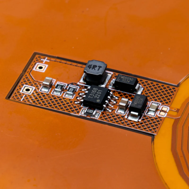
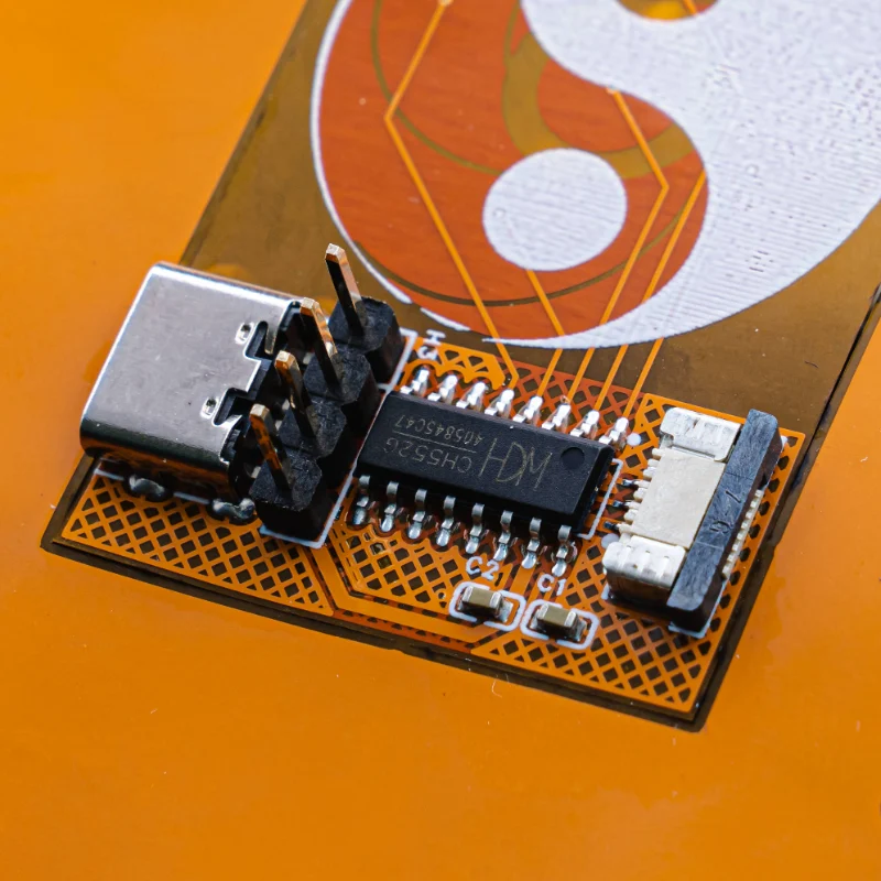
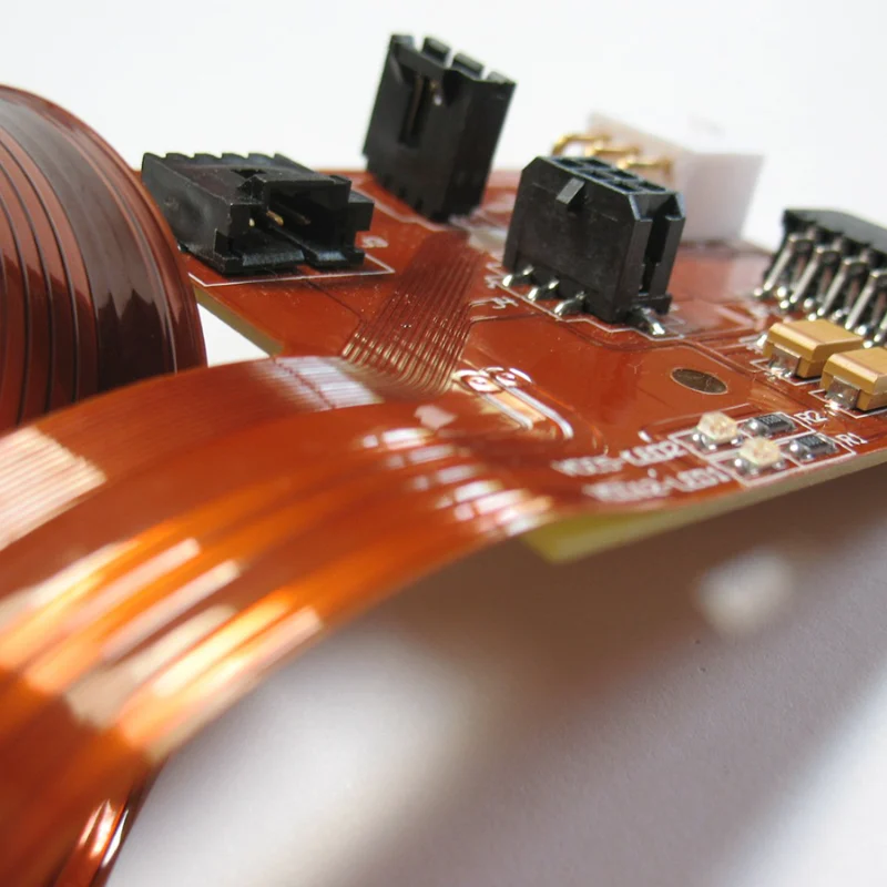
● Connectors and sockets: When these through-hole or large SMD components are soldered onto FPCs, localized stress concentrations can occur. A reinforcing plate (usually stainless steel or polyimide sheet) needs to be designed on the back of the FPC (below the corresponding component) and attached before or after reflow soldering to enhance mechanical strength and prevent pad detachment during use.
● Ultra-thin/miniature components: The amount of solder paste needs to be controlled to prevent bridging.
III. Summary:
● Excellent carrier design is the cornerstone of success, solving four major problems: positioning, support, flatness, and heat transfer.
● A gentle, customized reflow soldering profile is crucial for ensuring high yield. DOE (Design of Experiments) optimization must be performed based on the specific FPC material, thickness, and component layout.
● Gentle handling and a clean environment throughout the entire process are fundamental guarantees.
● Engineering Collaboration: SMT processes must work closely with FPC design (layout, pad design, reinforcement design) to create conditions for Design-Functional Manufacturing (DFM) from the design stage.
By systematically addressing the three inherent challenges of FPCs—flexibility, deformability, and poor heat resistance—its placement yield can reach a level comparable to rigid PCBs. This requires process engineers with extensive experience and meticulous attention to detail.
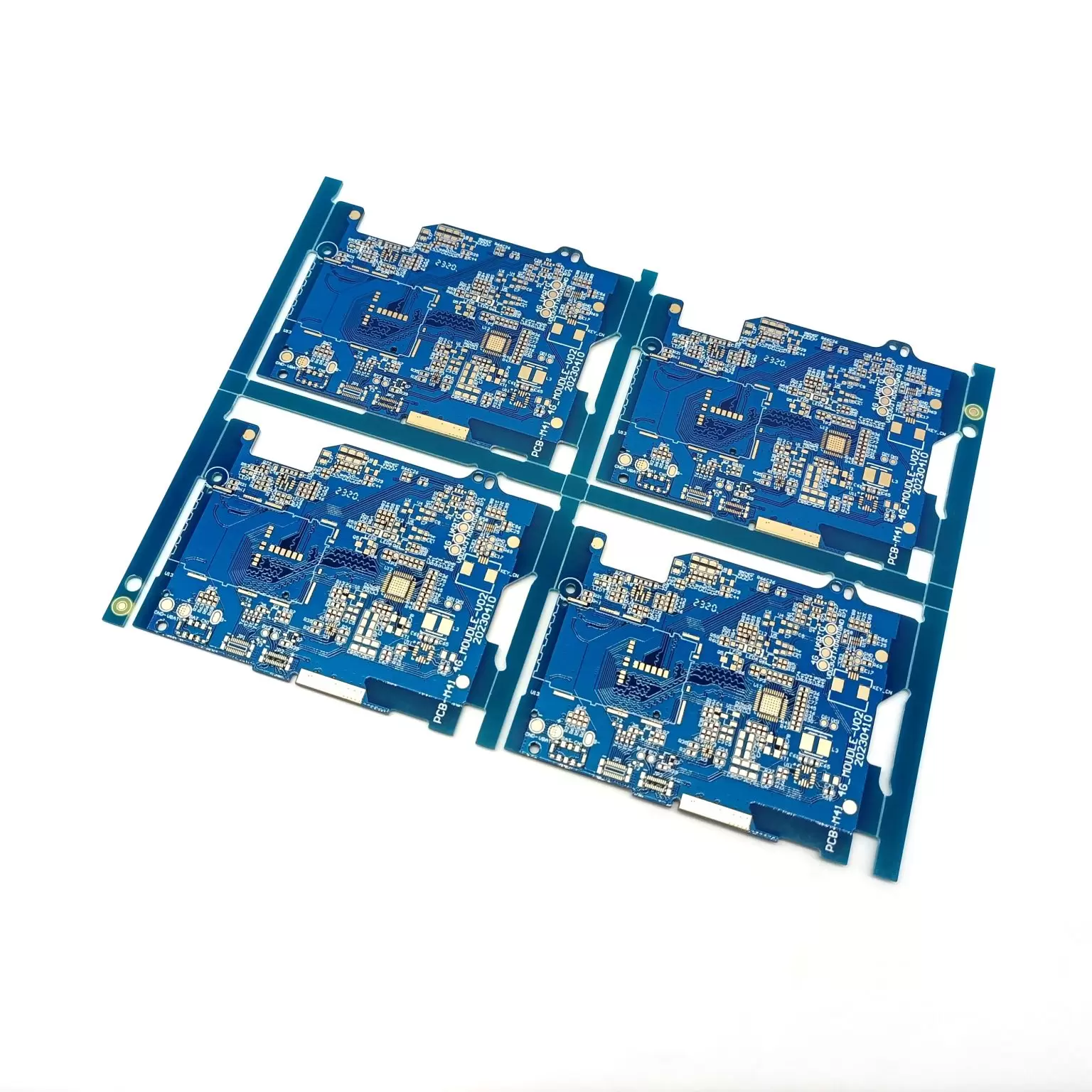
Benlida is a professional PCB&PCBA manufacturer, for over 14 years, with advanced equipment and experienced engineering team, Benlida is committed to providing top-class service to global customers. In addition to traditional PCB and PCBA, we have expanded into FPC production division and SMT assembly services. If you need FPC and assembly services, feel free to contact Benlida!
About the auther:

Sonic Yang
As a major of Electronics and Mechanical Automation, Sonic has been engaged in PCB design, R&D, manufacturing of eletronics for around 22 years, as engineering director and coordinates with supply chain(components&CNC parts), providing professional supports and consults for global customers.
 en
en

.jpg)

 WhatsApp