Medical pressure sensing equipment depends on electronic circuits that can capture small changes in pressure and convert them into stable, usable signals. The sensor itself may occupy only a small part of the system, but the PCB around it has a much broader responsibility. Power delivery, signal routing, grounding, component placement, thermal behavior, and solder joint quality all have a direct connection with the consistency of the finished electronic assembly.
For medical equipment manufacturers, this creates a practical engineering question: how should the PCB be built when the pressure sensor has to operate reliably inside a compact electronic system?
A conventional FR4 PCB remains suitable for many medical electronic products. It offers mature manufacturing processes, broad material availability, and a reasonable cost structure. Certain pressure sensing applications, however, place greater demands on thermal stability, circuit density, signal integrity, or long-term reliability. In these cases, Ceramic PCB technology can provide another option.
A Medical Pressure Sensor Electronic PCB Assembly brings the sensor circuit, substrate, components, and assembly process together as one manufacturing system. The quality of each part matters. A good sensor cannot compensate for poor signal routing, unstable power delivery, weak solder joints, or inadequate thermal management.
For this reason, PCB selection should begin with the operating conditions of the medical device rather than with material cost alone.
What Makes Medical Pressure Sensor PCB Assembly Different
Pressure sensors are used to detect changes that may be relatively small compared with the electrical activity generated elsewhere in the equipment. The PCB therefore needs to provide a stable environment for signal acquisition and processing.
A typical pressure sensing circuit may contain the sensor, signal conditioning components, amplifiers, converters, processors, power management components, and communication interfaces. Their physical arrangement on the PCB affects how the circuit behaves.
Three areas deserve particular attention.
Signal Stability
A pressure sensor PCB may need to process low-level signals before they reach a controller or processor. Unnecessary electrical noise can make signal processing more difficult and may affect measurement consistency.
PCB layout therefore needs to consider trace routing, grounding, power distribution, component positioning, and the relationship between sensitive signal paths and higher-current circuits.
The board material is only one part of this process. A well-selected substrate must be combined with an appropriate circuit layout and controlled assembly process.
For a Medical PCB Assembly, the manufacturing team should understand the function of each circuit area rather than treating every board as a standard production order.
Compact Circuit Layout
Medical equipment often places several electronic functions into a limited enclosure. The PCB may need to accommodate sensor interfaces, processing circuits, power components, and communication connections within a relatively small board area.
The product specifications provided for this project include a minimum line width of 3 mil, minimum line spacing of 3 mil, and a minimum hole size of 0.02 mm. These specifications indicate the level of precision available for custom PCB manufacturing, while the final parameters still need to be selected according to the actual circuit design.
A compact layout also makes component placement more important. Sensitive components should be positioned with their electrical and thermal environment in mind. Power devices, for example, may need to be kept away from circuits that require cleaner signal conditions.
Thermal Conditions
Heat is another factor that can affect electronic stability.
A pressure sensing module may operate alongside power conversion, processing, communication, or other electronic functions. Heat generated by these components can spread through the PCB and surrounding structure.
In a tightly packaged product, there may be limited room for conventional cooling methods. The PCB then becomes part of the thermal path.
This is one reason engineers may consider Ceramic PCB Assembly for applications where thermal performance is a significant design requirement.
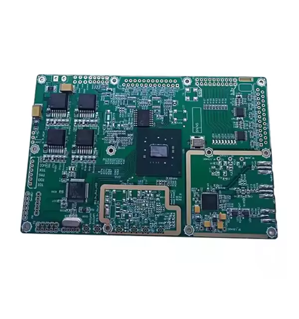
Why Ceramic PCB Can Benefit Medical Pressure Sensor Electronics
Ceramic PCB technology uses ceramic materials as the substrate instead of the fiberglass-based structure commonly associated with FR4.
The product information supplied for this application identifies FR4, aluminum, and ceramic among the available material options. Ceramic substrates can include materials such as alumina and aluminum nitride, with material selection depending on the electrical, thermal, mechanical, and manufacturing requirements of the project.
The most important reason to consider ceramic is thermal behavior.
Ceramic substrates can provide much higher thermal conductivity than standard FR4. The product information gives a reference of up to 220 W/m·K for ceramic PCB materials, compared with approximately 0.25 W/m·K for FR4. The actual value depends on the ceramic material and construction used for the specific PCB.
That difference matters when electronic components generate concentrated heat.
Instead of allowing heat to remain heavily concentrated around a component, a higher-conductivity substrate can help move thermal energy away from the heat source and toward other parts of the thermal management system.
For pressure sensor electronics, this can be useful when the sensor circuit shares space with components that generate more heat.
Thermal Management Around Sensitive Circuits
Good thermal management is not simply about keeping the PCB cool.
Temperature gradients across a compact electronic assembly can also affect component behavior and mechanical conditions. When a heat-generating component is placed close to a sensitive sensing circuit, the resulting thermal environment needs to be considered during PCB design.
A ceramic substrate gives engineers another material option when thermal transfer is important.
The result is not automatic. Ceramic PCB performance still depends on board construction, copper layout, component placement, heat paths, enclosure design, and the complete product structure.
That is why material selection should be made together with PCB design and assembly planning.
Electrical and Mechanical Considerations
Ceramic materials also offer strong electrical insulation characteristics and good dimensional stability for demanding electronic applications.
These properties can be valuable in compact sensor assemblies where board dimensions, circuit density, and long-term operating conditions all need to remain controlled.
For a Medical Sensor PCB, this can provide an additional level of design flexibility when FR4 does not offer enough thermal or dimensional performance for the intended application.
The decision should still be based on actual operating requirements. A low-power pressure sensor board with modest thermal demands may not need a ceramic substrate. A compact design with concentrated heat and stricter reliability requirements may justify the additional material and manufacturing cost.
Ceramic PCB or FR4 for Pressure Sensor Electronics
The choice between FR4 and ceramic should be made from the application requirements.
FR4 remains highly practical for many medical electronic assemblies. It has a mature supply chain and well-established PCB Manufacturing processes. For products where thermal loads are moderate and standard electrical performance is sufficient, FR4 can offer a sensible balance between performance and cost.
Ceramic PCB becomes more attractive when thermal management, dimensional stability, or high-reliability requirements become more demanding.
Factor | FR4 PCB | Ceramic PCB |
Substrate | Fiberglass reinforced epoxy | Ceramic material |
Thermal conductivity | Relatively low | Significantly higher depending on material |
Thermal management | Suitable for conventional loads | Suitable for demanding thermal conditions |
Manufacturing maturity | Very mature | Requires specialized processes |
Cost | Generally lower | Generally higher |
Typical role | General electronic circuits | High-performance and demanding electronic applications |
There is no single substrate that suits every Medical PCB Assembly project.
The better approach is to identify the pressure sensor's electrical requirements, heat generation, enclosure conditions, board dimensions, component density, expected operating environment, and target service life before selecting the material.
For a custom project, this assessment also helps determine whether a standard FR4 structure, aluminum PCB, or Custom Ceramic PCB provides the most appropriate solution.
PCB Layout Matters as Much as Material Selection
Selecting a high-performance substrate does not remove the need for careful PCB design.
For pressure sensor electronics, layout decisions can influence the behavior of the complete assembly.
Sensitive signal traces should have a suitable routing path. Grounding needs to be planned around the circuit architecture. Power traces must handle their expected current without creating unnecessary interference with sensitive sections.
Component placement also deserves attention.
A pressure sensor and its signal conditioning circuit may require a different electrical environment from a switching power supply or high-current driver. Keeping these functional areas properly arranged can help reduce unwanted coupling and make production easier to control.
For multilayer designs, the stack-up should also be considered during the engineering stage. Signal layers, power distribution, and ground structures need to work together rather than being treated as independent parts of the PCB.
These details become especially important when the board combines sensor signals with digital processing or communication functions.
A High Reliability PCB Assembly therefore depends on more than the selected substrate. Material, layout, fabrication, component selection, and SMT assembly all need to support the same reliability target.
How SMT Assembly Affects Medical Pressure Sensor PCB Reliability
The PCB substrate sets the foundation, but the assembly process determines how that board becomes a working electronic product.
For a Medical Pressure Sensor Electronic PCB Assembly, component placement, solder paste printing, reflow control, inspection, and handling all need to remain consistent from one production batch to the next. A small variation in assembly can become a larger problem after the board enters long-term operation.
Component Placement Accuracy
Pressure sensing circuits can contain small passive components, integrated circuits, sensor interfaces, and other compact devices. Their position on the board needs to match the PCB layout accurately.
Modern SMT equipment can place components at high speed while maintaining controlled placement accuracy. For a custom medical PCB project, however, equipment capability is only one part of the process. Component packages, pad design, feeder setup, PCB surface condition, and production parameters all affect the final result.
Correct placement also supports thermal management.
Heat-generating components need sufficient consideration during layout and assembly. When their locations are controlled according to the engineering design, the intended thermal paths are easier to maintain.
Solder Paste Printing
Solder paste printing is one of the first critical steps in SMT Assembly.
The amount of solder deposited onto each pad needs to correspond with the pad geometry and component package. Excess solder can create bridging or other defects, while insufficient solder may reduce joint quality.
For compact boards with fine-pitch components, stencil design and printing control become particularly important.
The supplied product specifications include a 3 mil minimum line width and 3 mil minimum line spacing. Boards using fine geometries require an assembly process capable of working consistently with the corresponding pad and component dimensions.
Reflow Soldering
The reflow profile also needs to match the components, solder materials, PCB construction, and production requirements.
A controlled temperature profile helps achieve consistent solder joint formation while limiting unnecessary thermal stress on components and the board.
For a Ceramic PCB Assembly, the material characteristics need to be considered during process development. Ceramic substrates behave differently from conventional FR4 structures, so the manufacturing team needs to establish suitable parameters rather than simply copying a standard FR4 production profile.
Inspection and Process Control
Inspection provides another layer of protection against assembly defects.
Depending on the PCB design, production requirements may include:
· Automated optical inspection
· Solder joint inspection
· X-ray inspection for selected packages
· Electrical testing
· Functional testing
The inspection strategy should match the actual product structure.
For a pressure sensor PCB, checking whether components are present is not enough. The finished assembly also needs to satisfy the electrical and functional requirements defined for the project.
Manufacturing Parameters That Matter
The technical specifications of a PCB influence both fabrication and assembly.
For the product supplied for this project, the listed specifications include a 1.6 mm board thickness and 10 oz copper thickness. The available surface finishes include HASL, OSP, and ENIG.
These parameters should not be selected independently.
Copper thickness, board thickness, line width, line spacing, hole size, component package, current requirements, and surface finish all need to work together with the PCB design.
Copper Thickness
The listed 10 oz copper specification provides a substantial copper layer for applications that require high current-carrying capability.
However, the appropriate copper thickness depends on the circuit. A pressure sensor signal circuit may have very different requirements from a power section located on the same assembly.
This distinction is important during engineering review.
A board should not be specified with heavy copper simply because thicker copper sounds more reliable. The actual current, heat generation, trace geometry, fabrication process, and component connections should determine the requirement.
Surface Finish
The product specifications support:
· HASL
· OSP
· ENIG
Each surface finish has its own manufacturing characteristics and application considerations.
ENIG, for example, is frequently selected when a flat surface and compatibility with fine-pitch components are important. HASL remains a mature and widely used option, while OSP provides another surface treatment choice for suitable PCB designs.
The final finish should be selected according to the component packages, assembly process, storage requirements, and project specifications.
When Should Engineers Consider a Ceramic PCB
Ceramic PCB should not automatically replace FR4 in every medical sensing product.
The decision makes more sense when the application has a clear requirement that ceramic material can address.
A ceramic substrate may deserve consideration when:
· Heat is concentrated in a small PCB area
· Thermal management is a major design concern
· The electronics operate under demanding temperature conditions
· Board dimensional stability is important
· Component density is high
· The product requires a higher reliability level
· The PCB has to combine sensitive circuits with heat-generating components
For a simple low-power pressure monitoring circuit, FR4 may remain a practical solution.
For a compact medical electronic system where thermal behavior becomes difficult to manage, a Custom Ceramic PCB can provide another engineering route.
The key is to compare the actual operating conditions with the physical characteristics of each substrate.
Selecting a Medical PCB Assembly Manufacturer
Material selection is only the beginning of the procurement process.
A medical equipment manufacturer evaluating a Medical PCB Assembly Manufacturer should look at the company's ability to manage the complete production chain.
PCB Manufacturing Capability
The manufacturer should be able to work with the required board thickness, copper thickness, line width, line spacing, hole dimensions, and surface finish.
The supplied specifications provide several examples of available manufacturing parameters:
· 1.6 mm board thickness
· 10 oz copper
· 0.02 mm minimum hole size
· 3 mil minimum line width
· 3 mil minimum line spacing
· HASL, OSP, and ENIG surface finishes
· FR4, aluminum, and ceramic material options
These capabilities provide a starting point for custom projects. The final production specification should always be confirmed against the actual PCB design and manufacturing requirements.
SMT Assembly Capability
PCB fabrication and component assembly are closely connected.
A supplier may produce the bare board correctly but still create problems during SMT production if placement, soldering, inspection, or testing is not properly controlled.
For a Medical Pressure Sensor Electronic PCB Assembly, the procurement team should therefore evaluate both PCB manufacturing and assembly capability.
A supplier with integrated production can also reduce communication gaps between board fabrication and assembly teams.
Customization
Medical pressure sensor systems vary considerably in circuit architecture and physical configuration.
Some designs may require conventional FR4. Others may need aluminum or ceramic substrates. Board dimensions, copper thickness, hole structure, surface finish, and component layout can also vary from one project to another.
For this reason, Custom PCB Assembly capability is important for OEM customers developing specialized medical electronic equipment.
The supplier should be able to review engineering files, evaluate manufacturability, identify potential production concerns, and confirm the practical parameters before mass production.
Reliability Starts Before Production
Long-term PCB reliability is determined well before the first finished board leaves the assembly line.
The engineering team needs to consider:
Material → PCB Design → Fabrication → SMT Assembly → Inspection → Testing
Each stage affects the next.
For a pressure sensor application, the goal is not simply to produce a board that powers on successfully. The finished assembly needs to maintain stable electrical connections and support consistent sensor operation throughout the intended service period.
Ceramic PCB can contribute to this goal when thermal performance is a major requirement. Careful PCB layout helps control signal and power relationships. A controlled SMT process protects component and solder joint quality. Inspection and testing then provide production verification.
This is where an experienced PCB Assembly Manufacturer can make a meaningful difference.
A Practical Approach to Medical Pressure Sensor PCB Projects
For OEMs developing pressure sensing equipment, the most effective approach is to begin with the application rather than choosing a PCB material first.
Start with the operating conditions:
· What temperature range will the electronics experience?
· Where are the major heat sources?
· How sensitive are the sensor signals?
· How much board space is available?
· What components need to be installed?
· What copper thickness is required?
· What level of circuit density is expected?
· How frequently will the equipment operate?
· What service life is expected?
The answers provide a basis for selecting FR4, aluminum, or ceramic materials.
From there, the PCB design and assembly process can be developed around the selected architecture.
For projects requiring higher thermal performance, a Ceramic PCB Manufacturer with PCB assembly capability can provide a more complete production route. For standard designs, FR4 may remain the more economical option.
The right solution is therefore not determined by material name alone. It comes from matching substrate properties, circuit design, manufacturing capability, and operating conditions.
A pressure sensor may be responsible for detecting a physical change, but the PCB assembly determines how reliably that information travels through the electronic system.
For medical equipment manufacturers, Medical Pressure Sensor Electronic PCB Assembly requires attention to signal stability, thermal conditions, component placement, solder quality, board construction, and long-term manufacturing consistency.
FR4 remains a practical material for many applications. Ceramic PCB becomes more relevant when thermal management, compact construction, and demanding reliability requirements place greater pressure on the board design.
With options covering FR4, aluminum, and ceramic materials, together with specifications such as 1.6 mm board thickness, 10 oz copper, 3 mil line width and spacing, 0.02 mm minimum hole size, and HASL, OSP, or ENIG surface finishes, custom PCB projects can be developed around the actual requirements of the electronic system.
For medical pressure sensing equipment, the strongest PCB solution is the one that balances signal integrity, thermal performance, manufacturability, assembly quality, and long-term reliability. That balance is what turns a PCB from a basic circuit carrier into a dependable part of a medical electronic system.
About the author:

Sonic Yang
As a major in Electronics and Mechanical Automation, Sonic has been engaged in PCB design, R&D, and manufacturing of electronics for around 22 years, as the engineering director, and coordinates with the supply chain(components and CNC parts), providing professional support and consulting for global customers.

 en
en





 WhatsApp