The Comprehensive Processes of Electric Vehicle PCB Assembly
As the global automotive industry accelerates toward electrification, the demand for high-performance, reliable printed circuit boards (PCBs) in electric vehicles (EVs) has surged. EV PCBs serve as the nervous system of critical systems—from battery management and motor control to infotainment and autonomous driving features. Unlike traditional automotive PCBs, EV variants must withstand higher voltages, extreme temperatures, and rigorous vibration, requiring specialized assembly processes. Below is a detailed breakdown of the key stages in electric vehicle PCB assembly.
1. Design for Manufacturability (DFM) and Prototyping
The assembly process begins long before physical production with rigorous design validation. EV PCB designs must account for:
· High-voltage compatibility: EV systems often operate at 400V-800V, demanding robust insulation and trace spacing to prevent arcing.
· Thermal management: Components like power inverters and battery management systems (BMS) generate significant heat, requiring thermal vias, aluminum cores, or heat sinks integrated into the PCB design.
· Vibration resistance: PCBs in EVs must endure constant mechanical stress from road conditions, necessitating secure component mounting and reinforced solder joints.
Engineers conduct DFM analysis to optimize layouts for manufacturability, identifying potential issues such as component accessibility, solder mask coverage, and drill hole placement. Prototypes are then produced using rapid fabrication techniques (e.g., 3D printing for enclosures, quick-turn PCB manufacturing) to test form, fit, and function. These prototypes undergo thermal cycling, vibration, and voltage stress tests to validate performance under real-world conditions.
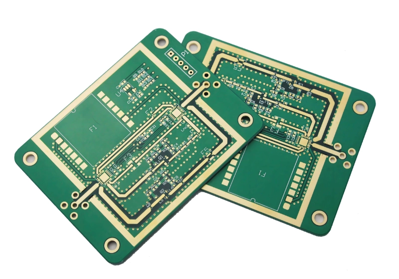
2. PCB Fabrication: Customized Substrates for EV Demands
EV PCBs require specialized substrates tailored to their operating environments:
· Material selection: High-temperature materials like FR-4 with enhanced Tg (glass transition temperature) or polyimide are used to withstand under-hood temperatures exceeding 125°C. For BMS and power modules, metal-core PCBs (MCPCBs) or aluminum-backed PCBs improve heat dissipation.
· Layer configuration: Complex EV systems (e.g., autonomous driving controllers) use high-layer count PCBs (12-24 layers) to accommodate dense components and high-speed signal paths. HDI (High-Density Interconnect) technology enables finer trace widths (down to 30μm) and microvias for compact designs.
· Surface finishes: Immersion silver or electroless nickel immersion gold (ENIG) finishes are preferred for their corrosion resistance and compatibility with lead-free soldering, critical for EVs exposed to moisture and road salts.
Fabrication involves precision etching, drilling, and plating to ensure signal integrity and mechanical strength. Each PCB undergoes initial testing (e.g., continuity checks, impedance testing) to verify compliance with design specifications.
3. Component Sourcing and Preparation
EV PCBs integrate a mix of standard and specialized components, including:
· Power semiconductors (IGBTs, MOSFETs) for motor controllers and inverters
· Sensors (temperature, current, pressure) for BMS and safety systems
· Microcontrollers and FPGAs for processing and control
· Connectors and terminals rated for high voltage and current
Sourcing prioritizes:
· Automotive-grade components: Parts must meet AEC-Q100 (integrated circuits) or AEC-Q200 (passive components) standards for reliability in harsh environments.
· Traceability: Full documentation of component origins, batch numbers, and test reports ensures compliance with automotive regulations (e.g., IATF 16949).
· Anti-counterfeit measures: Components are verified via X-ray inspection, laser marking analysis, and supplier audits to prevent counterfeit parts from entering the supply chain.
Before assembly, components are stored in ESD (electrostatic discharge) safe environments. Tape-and-reel packaging is used for SMT (Surface Mount Technology) components to enable automated placement, while larger through-hole components (e.g., high-power connectors) are prepared for wave soldering.
4. Assembly: Precision Techniques for EV Reliability
EV PCB assembly combines advanced automation with rigorous quality checks to meet automotive standards:
a. SMT Assembly for Miniaturized Components
· Solder paste application: Stencils with laser-cut apertures deposit solder paste onto PCB pads with micron-level precision. For fine-pitch components (e.g., BGA packages in ADAS controllers), 3D solder paste inspection (SPI) verifies paste volume and alignment.
· Component placement: High-speed pick-and-place machines (capable of placing 50,000+ components per hour) mount SMT parts, using vision systems to align components with tolerances as tight as ±5μm. This is critical for high-density areas like battery management PCBs, where misalignment could cause short circuits.
· Reflow soldering: PCBs pass through a reflow oven with a controlled temperature profile (peak temperatures up to 260°C for lead-free solder) to melt the paste and form strong solder joints. Thermal profiling ensures components (especially heat-sensitive sensors) are not damaged during soldering.
b. Through-Hole and Power Component Assembly
· Wave soldering: For through-hole components (e.g., power terminals, fuses), PCBs are passed over a wave of molten solder, which fills the holes and forms joints. This is common in high-current PCBs for motor controllers.
· Selective soldering: Automated robots apply solder to specific through-hole components, reducing thermal stress on nearby SMT parts—a technique used for mixed-technology PCBs in charging systems.
· Press-fit technology: For high-reliability connections (e.g., connectors in battery packs), press-fit pins are mechanically inserted into plated holes, eliminating the need for solder and reducing the risk of cold joints.
c. Advanced Processes for Power Modules
EV power PCBs (e.g., inverter boards) require additional steps:
· Die bonding: Bare semiconductor dies (e.g., SiC or GaN chips for high-efficiency inverters) are attached to heat sinks using conductive adhesives or solder, ensuring efficient heat transfer.
· Wire bonding: Ultrasonic welding connects die pads to PCB traces with fine aluminum or copper wires (25-50μm diameter), enabling high-current flow in compact spaces.
5. Inspection and Testing: Ensuring Zero Defects
EV PCBs undergo rigorous testing to meet safety-critical standards:
· Automated Optical Inspection (AOI): High-resolution cameras check for solder defects (bridges, cold joints), component misalignment, and missing parts.
· X-ray Inspection: Used to inspect hidden joints (e.g., BGA, CSP, or stacked die packages) for voids or incomplete wetting, critical for power semiconductors.
· In-Circuit Testing (ICT): Probes verify the functionality of individual components, checking for shorts, opens, and incorrect values.
· Functional Testing (FCT): PCBs are mounted in test fixtures that simulate real operating conditions (e.g., applying high voltage to BMS boards or testing motor controller response times).
· Environmental Stress Testing: Samples undergo thermal cycling (-40°C to 125°C), vibration testing (per ISO 16750), and humidity testing to validate long-term reliability.
6. Conformal Coating and Final Assembly
To protect against moisture, dust, and chemical exposure (e.g., road salts), EV PCBs are coated with:
· Conformal coatings: Silicone, acrylic, or urethane coatings are applied via spraying or dipping, forming a thin protective layer while allowing heat dissipation.
· Potting: For extreme environments (e.g., battery pack PCBs), epoxy potting compounds fully encapsulate the PCB, providing mechanical and chemical protection.
Finally, PCBs are integrated into larger assemblies (e.g., control modules, inverter housings) with connectors, heat sinks, and shielding. Each finished unit undergoes final functional testing before shipment to automotive OEMs.
Conclusion
Electric vehicle PCB assembly is a complex, precision-driven process that combines advanced materials, automated manufacturing, and stringent testing to meet the unique demands of EV systems. As EV technology evolves—with higher voltages, faster charging, and more autonomous features—assembly processes will continue to advance, emphasizing thermal management, high-power handling, and zero-defect reliability. By adhering to these rigorous processes, manufacturers ensure that EV PCBs not only perform flawlessly but also contribute to the safety, efficiency, and longevity of electric vehicles.
 en
en


 WhatsApp