Medical electronic equipment rarely follows one standard hardware configuration. A patient monitoring device, diagnostic instrument, portable medical system, laboratory instrument, or pressure sensing product can have very different requirements for board size, component density, power distribution, signal routing, thermal performance, and assembly.
That makes the PCB more than a platform for connecting electronic components. It becomes part of the engineering structure of the equipment.
A standard PCB specification may work well for one product and create unnecessary limitations for another. Board thickness, copper thickness, hole size, line width, line spacing, surface finish, substrate material, and component arrangement all need to match the circuit and the operating environment.
This is where Custom Medical PCB Assembly becomes valuable.
A custom approach allows the PCB fabrication and assembly process to follow the requirements of the actual medical electronic system. FR4 can remain a practical choice for many conventional circuits, while aluminum or ceramic substrates can be considered when thermal conditions become more demanding.
For manufacturers developing specialized medical electronics, the important question is not simply which PCB material is available. The better question is whether the PCB structure, manufacturing process, and assembly method are appropriate for the equipment being developed.
What Makes Medical PCB Assembly Different
Medical electronics place a strong emphasis on stable operation. A circuit board may need to remain functional for long periods while handling sensor signals, power conversion, data communication, processing, or multiple functions within a compact enclosure.
The requirements vary according to the equipment, but several areas usually deserve attention.
Signal Routing and Electrical Stability
Many medical devices contain sensors and signal acquisition circuits that work with relatively sensitive electrical signals. The PCB layout needs to keep signal paths, grounding, and power distribution under control.
Trace routing is particularly important when sensitive circuits share a board with switching power supplies, processors, communication interfaces, or other sources of electrical noise.
A suitable PCB design can separate functional areas and establish appropriate routing paths before production begins.
For Medical PCB Assembly, this means the manufacturing process should follow the engineering intent of the board design. Component placement, soldering, and inspection all need to remain consistent with the original design.
Compact Circuit Integration
Medical equipment often has limited internal space.
A PCB may need to accommodate sensors, processors, connectors, power components, and communication circuits within a relatively small area. Higher circuit density places greater demands on fabrication accuracy and assembly capability.
The product specifications provided for this PCB include a minimum line width of 3 mil, minimum line spacing of 3 mil, and a minimum hole size of 0.02 mm.
These figures represent available manufacturing specifications rather than a universal requirement for every medical PCB. The actual values should be selected according to the circuit layout, component package, electrical requirements, and production process.
Thermal Conditions
Heat becomes more relevant when several electronic functions share a compact enclosure.
Processors, power components, and other active devices can generate localized heat. If the heat path is poorly planned, nearby components may operate under less favorable thermal conditions.
PCB material and copper structure can contribute to thermal management, but they are only part of the complete solution. Component placement, copper distribution, thermal vias, enclosure design, and external cooling arrangements may also affect the final result.
For projects with higher thermal requirements, ceramic PCB technology provides another material option.
Why Customization Matters in Medical PCB Assembly
A medical PCB does not have to follow a fixed combination of dimensions and materials.
One product may need a conventional FR4 board with a compact multilayer structure. Another may require heavier copper because of current requirements. A different design may place greater emphasis on thermal conductivity and consider ceramic as the substrate.
This is why customization matters.
Board Thickness
The supplied product specification lists a 1.6 mm board thickness.
Board thickness affects mechanical structure, connector compatibility, enclosure integration, and the overall PCB construction. The correct thickness depends on the finished equipment and the requirements of the board design.
Copper Thickness
The listed copper thickness is 10 oz.
Copper thickness needs to be evaluated according to current requirements, trace geometry, thermal considerations, and fabrication capability. A medical PCB can contain both low-level signal circuits and higher-current power sections, so the copper requirement may differ between designs.
Hole Size and Circuit Density
The available minimum hole size is 0.02 mm, while the listed minimum line width and line spacing are both 3 mil.
Fine PCB geometries can provide greater layout flexibility, but they also require appropriate manufacturing control. A supplier needs to confirm that the selected dimensions are compatible with the complete PCB structure and production process.
The purpose of tighter specifications is not simply to make a PCB appear more advanced. They should solve a real layout or packaging requirement.
Surface Finish
The product supports HASL, OSP, and ENIG surface finishing.
Surface finish selection should follow the component package, assembly process, expected storage conditions, and project requirements.
For fine-pitch components, for example, surface flatness can become an important consideration. The final choice should therefore be made during engineering review rather than selected only according to material preference.
When Does Ceramic PCB Make Sense for Medical Electronics
Ceramic PCB is not necessary for every medical electronic product.
FR4 remains a widely used PCB material for conventional electronic circuits, particularly when thermal loads are moderate and standard PCB manufacturing processes provide sufficient performance.
Ceramic becomes more relevant when the electronic system has a stronger need for thermal performance or other properties associated with ceramic substrates.
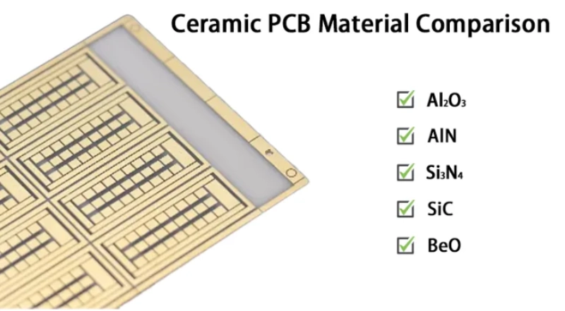
The product information supplied for this project identifies Alumina, Aluminum Nitride, and Silicon Carbide as ceramic substrate options and states thermal conductivity of up to 220 W/m·K for ceramic PCB materials.
The actual thermal conductivity depends on the selected ceramic material and construction.
High Thermal Loads
A compact electronic assembly may contain components that generate substantial localized heat. When the available space for conventional cooling is limited, substrate thermal performance becomes part of the design discussion.
Ceramic PCB can provide a higher thermal conductivity route than conventional FR4, making it relevant for electronic systems where heat transfer is a major engineering concern.
Compact High-Density Electronics
When more functions are placed into a smaller enclosure, heat and electrical performance need to be considered together.
A ceramic substrate can support thermal management while maintaining the electrical insulation required by the circuit structure.
This does not mean that every high-density medical PCB requires ceramic material. The selection should follow the actual heat generation, component arrangement, operating conditions, and reliability target.
Demanding Operating Conditions
Medical equipment may be expected to operate consistently over long periods. In applications with more demanding thermal conditions, substrate stability becomes part of the overall reliability discussion.
Ceramic PCB therefore provides another engineering option when the performance available from a conventional FR4 structure is not sufficient for the intended application.
Ceramic PCB Compared With FR4
Material selection should be based on application requirements rather than the assumption that one substrate is suitable for every medical device.
Factor | FR4 PCB | Ceramic PCB |
Substrate | Fiberglass reinforced epoxy | Ceramic material |
Thermal conductivity | Relatively low | Higher depending on ceramic material |
Manufacturing | Highly established | Requires specialized manufacturing capability |
Cost | Generally lower | Generally higher |
Thermal applications | Conventional thermal loads | Higher thermal management requirements |
Typical selection | General electronic applications | Demanding electronic and thermal applications |
FR4 can remain the more practical option when the medical device has moderate power consumption, conventional operating conditions, and no major thermal limitation.
Ceramic PCB becomes more attractive when thermal management, compact construction, or demanding operating conditions become important design factors.
The correct choice therefore starts with the product specification, not the substrate name.
How PCB Design Affects Custom Medical PCB Assembly
Selecting the PCB material is only one part of the engineering process. The circuit layout has a direct effect on how the finished board performs after assembly.
For Custom Medical PCB Assembly, PCB design needs to consider electrical connections, component placement, heat distribution, mechanical dimensions, and the manufacturing process at the same time. A board may meet the basic schematic requirements but still create manufacturing difficulties if the physical layout does not match the production capability.
Signal Routing and Grounding
Medical electronic systems may contain sensor circuits, processors, communication interfaces, power supplies, and other functions on the same board. These circuits can have different electrical characteristics.
Sensitive signal paths should be planned carefully so that unnecessary interference is minimized. Ground structures and power distribution also need to follow the circuit architecture.
For multilayer boards, the layer arrangement can affect signal routing and power distribution. Component placement should support the intended current paths and keep related circuit functions properly grouped.
These decisions are made during PCB design, but their impact continues into PCB Assembly.
Component Placement
Component placement affects both electrical performance and manufacturing efficiency.
High-power components may require greater spacing or additional thermal consideration. Sensitive components may need to remain away from potential noise sources. Connectors need to align with the mechanical structure of the finished equipment.
At the same time, components need to remain accessible to the selected SMT process.
A good PCB layout therefore considers both the electrical design and the assembly process before production starts.
Thermal Layout
Thermal management should be considered at the PCB design stage rather than treated as a problem after assembly.
Copper areas, thermal vias, component spacing, and the location of heat-generating devices can all influence how heat moves through the board.
When a ceramic substrate is selected, its thermal characteristics become another part of this design calculation.
For applications requiring higher thermal conductivity, Ceramic PCB Assembly can provide a different thermal path from conventional FR4 construction. The actual result still depends on the complete board design and the thermal characteristics of the selected ceramic material.
How SMT Assembly Supports Custom Medical PCB Production
After PCB fabrication, the assembly process determines how components are installed onto the board.
For medical electronics, consistent assembly is important because soldering defects, component placement errors, and insufficient inspection can affect finished-product reliability.
A typical SMT process may include several controlled stages.
Solder Paste Printing
Solder paste must be deposited onto the correct PCB pads with suitable volume and alignment.
The stencil design should match the component packages and PCB layout. Fine-pitch devices place greater demands on printing accuracy.
The listed 3 mil minimum line width and 3 mil minimum line spacing provide an example of the fine geometry that may be required in a custom PCB project. The assembly process still needs to be developed around the actual component package and pad structure.
Component Placement
Automated placement equipment installs components according to the programmed PCB design.
Placement accuracy matters for small components and fine-pitch devices. Feeder configuration, component orientation, PCB positioning, and machine calibration all contribute to the finished assembly.
For a Custom Medical PCB Assembly project, component placement should also be checked against the mechanical requirements of the final medical device.
Reflow Soldering
After component placement, the PCB passes through a controlled reflow process.
Temperature settings and heating stages need to correspond with the solder materials, components, PCB structure, and production requirements.
The objective is to form consistent solder joints without exposing components or the PCB structure to unnecessary thermal stress.
Ceramic substrates may require process evaluation because their physical characteristics differ from conventional FR4 materials. Production parameters should therefore be confirmed during engineering preparation.
Inspection and Testing
PCB assembly does not end when soldering is completed.
Inspection and testing provide important production controls for identifying assembly problems before the finished board reaches the next stage of manufacturing.
Depending on the product and engineering requirements, inspection may include:
· Automated optical inspection
· Solder joint inspection
· X-ray inspection
· Electrical testing
· Functional testing
The appropriate combination depends on the board structure and product requirements.
For example, visual inspection can identify certain component placement and soldering issues, while X-ray inspection can provide additional information for solder joints that cannot be evaluated effectively from the surface.
Electrical and functional testing then addresses whether the finished assembly operates according to the specified circuit requirements.
For medical electronics, the test strategy should be established according to the actual product rather than applied as a generic checklist.
Manufacturing Parameters Need to Match the PCB Design
The specifications of a PCB are connected.
Board thickness, copper thickness, hole dimensions, line width, line spacing, surface finish, and material selection should be considered together.
The product information provided for this Custom Medical PCB Assembly includes:
Parameter | Listed Specification |
Base material | FR4 |
Board thickness | 1.6 mm |
Copper thickness | 10 oz |
Minimum hole size | 0.02 mm |
Minimum line width | 3 mil |
Minimum line spacing | 3 mil |
Surface finishing | HASL / OSP / ENIG |
Board size | Optional |
Material options | FR4 / aluminum / ceramic CEM1 |
Solder mask | White / black / yellow / green / red |
Silkscreen | Customized |
These specifications provide manufacturing options for custom projects. They should not be interpreted as a fixed configuration for every medical PCB.
For example, 10 oz copper may be relevant to a design with substantial current or thermal requirements, while a low-power medical sensing circuit may have very different copper requirements.
The same principle applies to board thickness, hole size, and circuit geometry.
Custom PCB Assembly for Different Medical Devices
Medical electronics cover a wide range of products, so PCB requirements can vary significantly.
A compact monitoring device may prioritize small dimensions and low power consumption. A diagnostic system may contain multiple processing and communication functions. A medical power module may place greater emphasis on current handling and heat dissipation.
This is where Custom PCB Assembly becomes more useful than selecting a standard board configuration.
Patient Monitoring Equipment
Monitoring equipment may combine sensors, processing circuits, displays, communication interfaces, and power management on a limited PCB area.
The board needs to accommodate these functions while maintaining appropriate signal routing and component placement.
Diagnostic Equipment
Diagnostic systems can contain more complex electronic structures and may require multiple PCB assemblies working together.
The PCB manufacturer needs to follow the customer's design files and manufacturing specifications while maintaining consistent fabrication and assembly quality.
Portable Medical Electronics
Portable products place additional emphasis on board size, weight, power consumption, and mechanical integration.
A compact PCB may require higher circuit density and carefully planned component placement.
Laboratory and Analytical Equipment
Laboratory equipment can operate for extended periods and may contain sensors, control circuits, motors, heaters, or communication modules.
Thermal conditions and long-term operating stability can become important considerations when selecting the PCB structure.
When a Ceramic PCB Assembly Becomes a Practical Choice
Ceramic material deserves consideration when the PCB has requirements that conventional FR4 cannot comfortably address.
The product information supplied for this project identifies ceramic materials including Alumina, Aluminum Nitride, and Silicon Carbide.
These materials can provide higher thermal conductivity than conventional FR4, although the actual performance depends on the specific ceramic substrate selected.
A ceramic solution may be considered when:
· Heat generation is concentrated around specific components
· Available PCB space limits conventional cooling methods
· Thermal conductivity is an important design parameter
· The electronic system operates under demanding conditions
· High reliability is required over extended operation
· The PCB needs to combine electrical insulation with efficient heat transfer
The decision should still be made through engineering evaluation.
For many conventional medical electronic products, FR4 remains a sensible and economical material. Ceramic PCB becomes more relevant when thermal and operating requirements justify the additional material and manufacturing cost.
What Buyers Should Check With a PCB Assembly Manufacturer
For OEMs purchasing Medical PCB Assembly, price is only one part of supplier evaluation.
A capable supplier should be able to discuss the PCB from both manufacturing and assembly perspectives.
Material Capability
The supplier should be able to confirm which materials can actually be manufactured and assembled.
For a custom medical project, this may include FR4, aluminum, or ceramic options.
PCB Manufacturing Capability
The buyer should verify whether the manufacturer can consistently produce the required:
· Board thickness
· Copper thickness
· Hole dimensions
· Line width
· Line spacing
· Surface finish
· Board size
The manufacturer's stated minimum capability is useful, but production consistency is equally important.
SMT Assembly Capability
PCB fabrication and assembly should be evaluated together when the project requires a finished PCB assembly.
The supplier should have suitable SMT equipment, process control, inspection methods, and testing capability for the component packages used in the design.
Engineering Communication
Custom projects often involve questions about manufacturability.
A supplier needs to communicate clearly when a particular PCB specification, component package, material combination, or assembly method requires further engineering review.
This is particularly useful during prototype development, when changes can still be made before mass production.
Why Manufacturing Consistency Matters
A medical electronic product may require hundreds or thousands of PCB assemblies over its production life.
A successful prototype is only the first step.
The manufacturing process needs to reproduce the same PCB structure, component placement, solder quality, and electrical performance across production batches.
This requires consistency in PCB fabrication, material handling, SMT placement, soldering, inspection, and testing.
For OEM customers, this consistency can be more valuable than simply achieving an impressive specification on one prototype.
A supplier capable of producing a 3 mil line width, for example, also needs to maintain that design requirement consistently throughout production according to the agreed manufacturing tolerance.
The same principle applies to copper thickness, hole dimensions, board thickness, and assembly quality.
Building a Custom Medical PCB Around the Actual Product
The most practical way to develop a medical PCB is to start from the equipment requirements.
The engineering team should first identify:
1. Electrical requirements
2. Thermal conditions
3. Mechanical dimensions
4. Component types and packages
5. Current requirements
6. Signal characteristics
7. Expected operating conditions
8. Production volume
9. Inspection and testing requirements
The PCB structure can then be developed around these conditions.
For a conventional low-power medical circuit, FR4 may provide sufficient performance and manufacturing flexibility.
For a product with greater thermal demands, aluminum or ceramic may be evaluated.
For a compact design with higher circuit density, finer line width and spacing may become relevant.
There is no single PCB configuration that fits every medical electronic product.
Custom Medical PCB Assembly is fundamentally about matching PCB engineering and manufacturing to the requirements of the medical device.
Board material, thickness, copper structure, circuit geometry, surface finish, component placement, SMT processing, inspection, and testing all contribute to the performance of the finished assembly.
The supplied product supports FR4, aluminum, and ceramic material options, with listed manufacturing capabilities including 1.6 mm board thickness, 10 oz copper, 0.02 mm minimum hole size, 3 mil minimum line width and spacing, and HASL, OSP, or ENIG surface finishing.
For standard medical electronics, FR4 may provide a practical balance between performance and manufacturing cost. When thermal management becomes a major engineering concern, ceramic PCB can provide another route, with materials such as Alumina, Aluminum Nitride, and Silicon Carbide available for different requirements.
For OEMs and medical equipment manufacturers, the right Medical PCB Assembly Manufacturer should therefore be evaluated on more than a single specification or quotation. PCB fabrication capability, material selection, SMT Assembly, inspection, testing, engineering communication, and production consistency all need to be considered together.
A well-matched custom PCB gives the medical device manufacturer greater control over the electronic architecture from the first prototype through volume production.
About the author:

Sonic Yang
As a major in Electronics and Mechanical Automation, Sonic has been engaged in PCB design, R&D, and manufacturing of electronics for around 22 years, as the engineering director, and coordinates with the supply chain(components and CNC parts), providing professional support and consulting for global customers.

 en
en



 WhatsApp