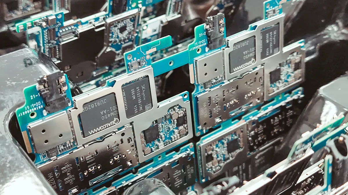
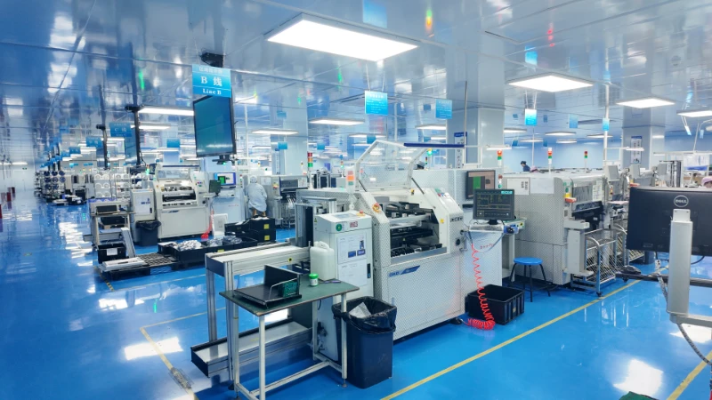
PCB assembly for internet devices forms the backbone of modern connectivity. The assembly process ensures strong electrical connections, which support stable communication and power efficiency in connected devices. Many Internet of Things products rely on precise assembly to keep data flowing smoothly.
●Quality control during PCB assembly prevents issues like signal loss and overheating.
●Designers must choose protocols such as Bluetooth or WiFi to optimize wireless performance.
Consistent assembly also guarantees predictable results when IoT devices are deployed on a large scale.
PCB Assembly for Internet Devices
Integration of Communication Modules
PCB assembly for internet devices centers on the need for seamless and reliable communication. Engineers design these boards to support a range of wireless technologies, which are essential for keeping IoT devices connected in real time. The integration of communication modules is a key part of this process. These modules allow devices to send and receive data, interact with networks, and operate within smart environments.
Common communication modules integrated into PCBs for internet devices include:
●Wi-Fi, which enables high-speed wireless networking.
●Bluetooth, used for short-range connections between devices.
●ZigBee, which forms mesh networks for low-power communication.
●LoRa, designed for long-range, low-power data transfer.
●Satellite communication, which supports connections over large distances.
●RFID, used for wireless identification and tracking.
●Z-Wave, popular in smart home systems for low-power control.
The assembly process must ensure that each module works without interference from others. Proper planning during PCB assembly allows for seamless connectivity and interoperability between different communication technologies. Engineers test wireless PCBs in various IoT devices to confirm that each module functions effectively in different environments.
A well-designed PCB assembly supports high-speed signal transmission, low signal loss, and effective EMI (electromagnetic interference) mitigation. These aspects are critical for real-time communication and data integrity. The table below summarizes how PCB assembly facilitates the integration of wireless modules:
Aspect | Description |
|---|
High-speed signal transmission | Essential for real-time communication in IoT devices, enabling data transfer to cloud systems. |
Low signal loss | Critical for maintaining the integrity of data being transmitted wirelessly. |
EMI mitigation | Reduces interference, ensuring reliable performance of wireless modules in compact designs. |
By focusing on layout consistency and clear signal paths, PCB assembly for internet devices helps maintain stable connections and predictable performance.
Control and Peripheral Interfaces
In addition to communication modules, PCB assembly must support a variety of control and peripheral interfaces. These interfaces connect the main board to sensors, actuators, and other components, allowing IoT devices to interact with their surroundings. The choice of interface depends on the device’s function and the type of data it needs to handle.
Some common control and peripheral interfaces found in connected devices include:
Interface Type | Function |
|---|
Modular Jack Panel | Connects pcbs to local area networks (LANs) and the Internet. |
Fiber Optic Patch Panel | Enables high-speed data transfer using light, ideal for noisy environments. |
Simple Communication Circuits | Facilitates basic data exchange over short distances. |
I2C (Inter-Integrated Circuit) | Allows multiple ICs to connect using minimal lines, useful for sensors and small modules. |
SPI (Serial Peripheral Interface) | Offers faster data transfer with additional lines, commonly used in microcontrollers. |
UART (Universal Asynchronous Receiver-Transmitter) | Used for direct device-to-device communication, one bit at a time. |
Ethernet | Connects devices to networks, managing data transfer efficiently. |
Fiber Optic Protocols | Transmits data over long distances using light, reducing electrical interference. |
Each interface requires careful placement and routing during PCB assembly. Consistent layout and signal continuity are vital for stable operation. If the assembly process introduces even minor variations, it can lead to unstable connections or unpredictable device behavior.
Note: Engineers pay close attention to the interaction between communication modules and control interfaces. This approach helps prevent interference and ensures that all parts of the system work together smoothly.
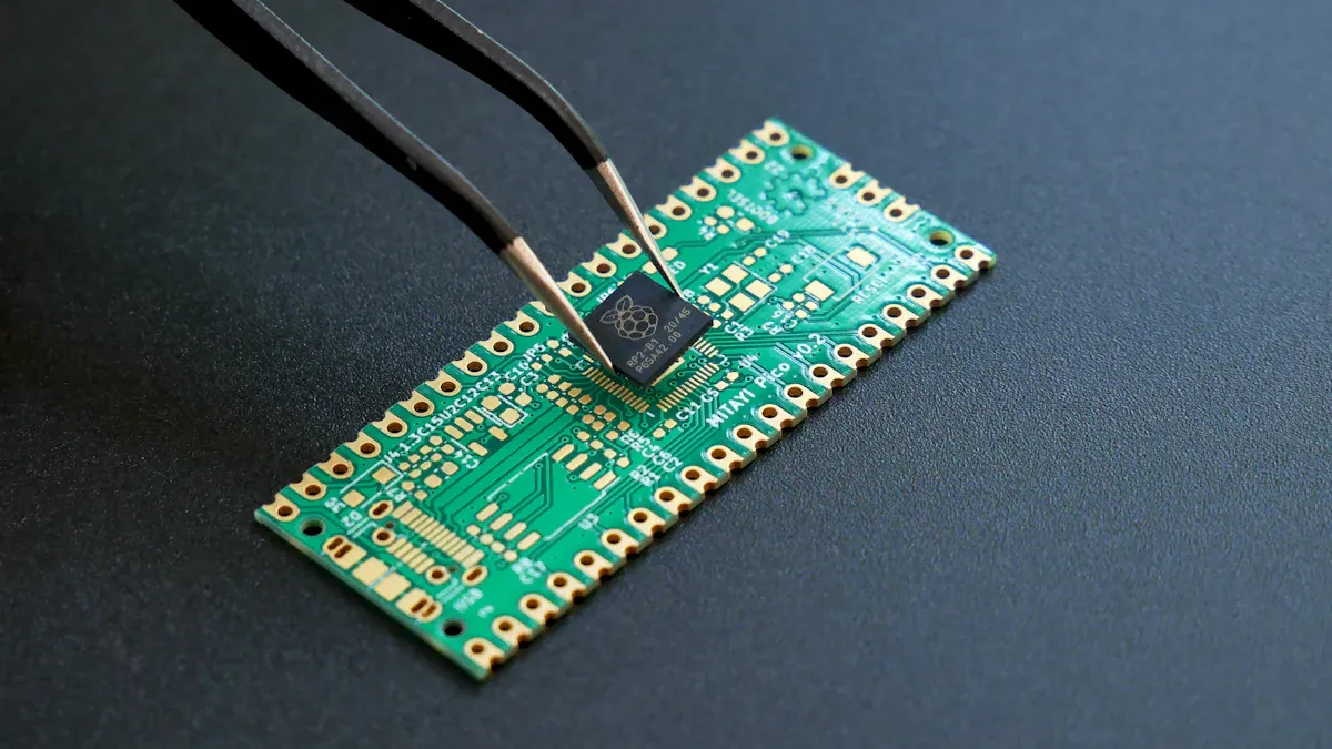
Miniaturization in IoT Devices
Compact PCB Layouts
Miniaturization has become a defining trend in the design of connected products. Engineers now create circuit boards that fit advanced features into very small spaces. This approach allows manufacturers to build smaller, lighter, and more portable devices.
In the IoT industry, it’s crucial for PCB designers to stay updated with the latest developments. New sensors, advanced board materials, and interface paradigms are consistently emerging.
Compact PCB layouts help reduce the distance that signals must travel. Shorter paths improve signal quality and lower the risk of data loss. The use of advanced materials also supports better performance in challenging environments. As devices shrink, every millimeter of space matters. Designers must plan the placement of each component with great care.
The table below shows how miniaturization affects device performance and reliability:
Aspect | Effect on Performance and Reliability |
|---|
Higher Performance | Shorter signal paths and reduced parasitic effects improve signal integrity and reduce losses, enhancing overall performance. |
Reliability and Testing | Thorough testing is essential to ensure functionality and reliability under real-world conditions, addressing potential defects. |
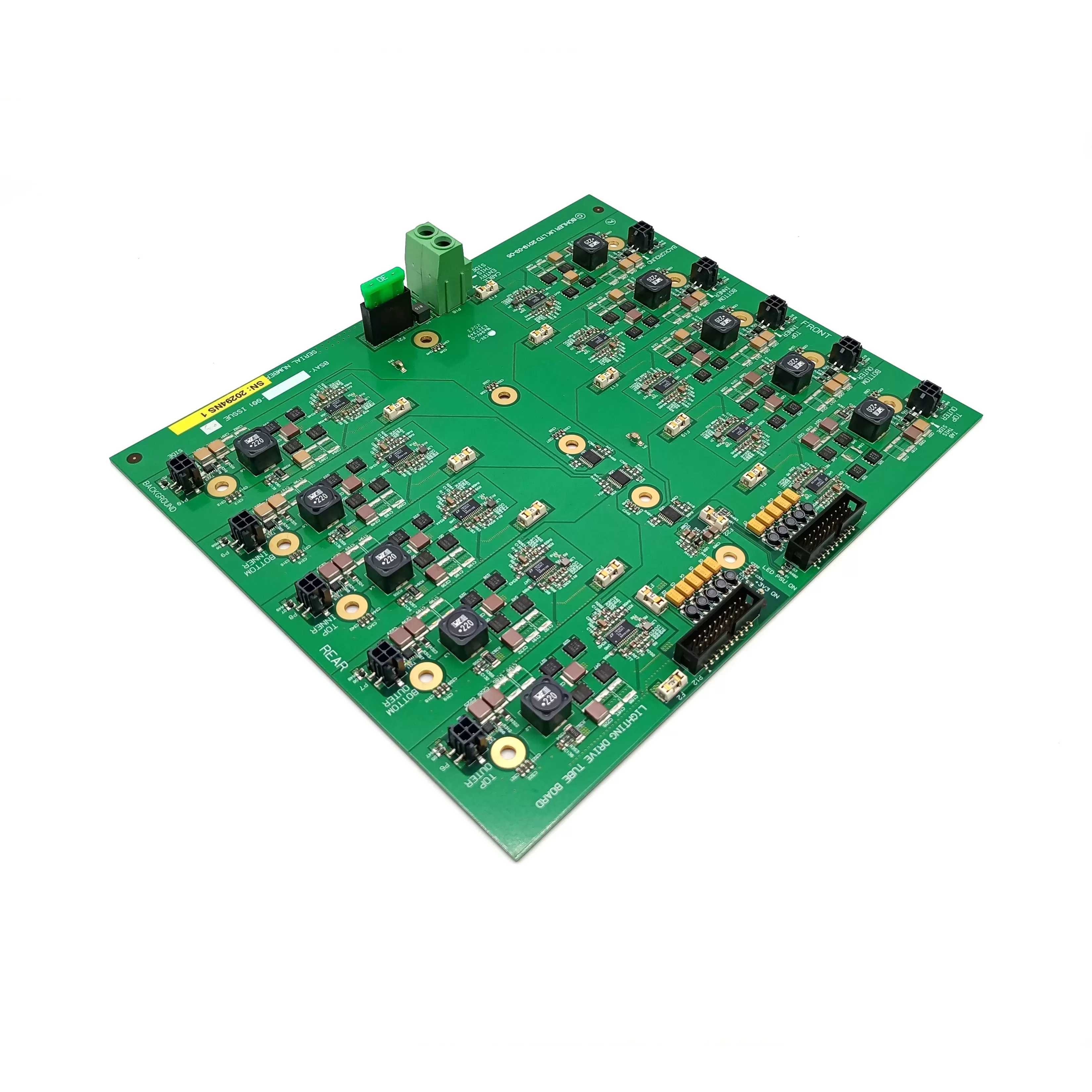
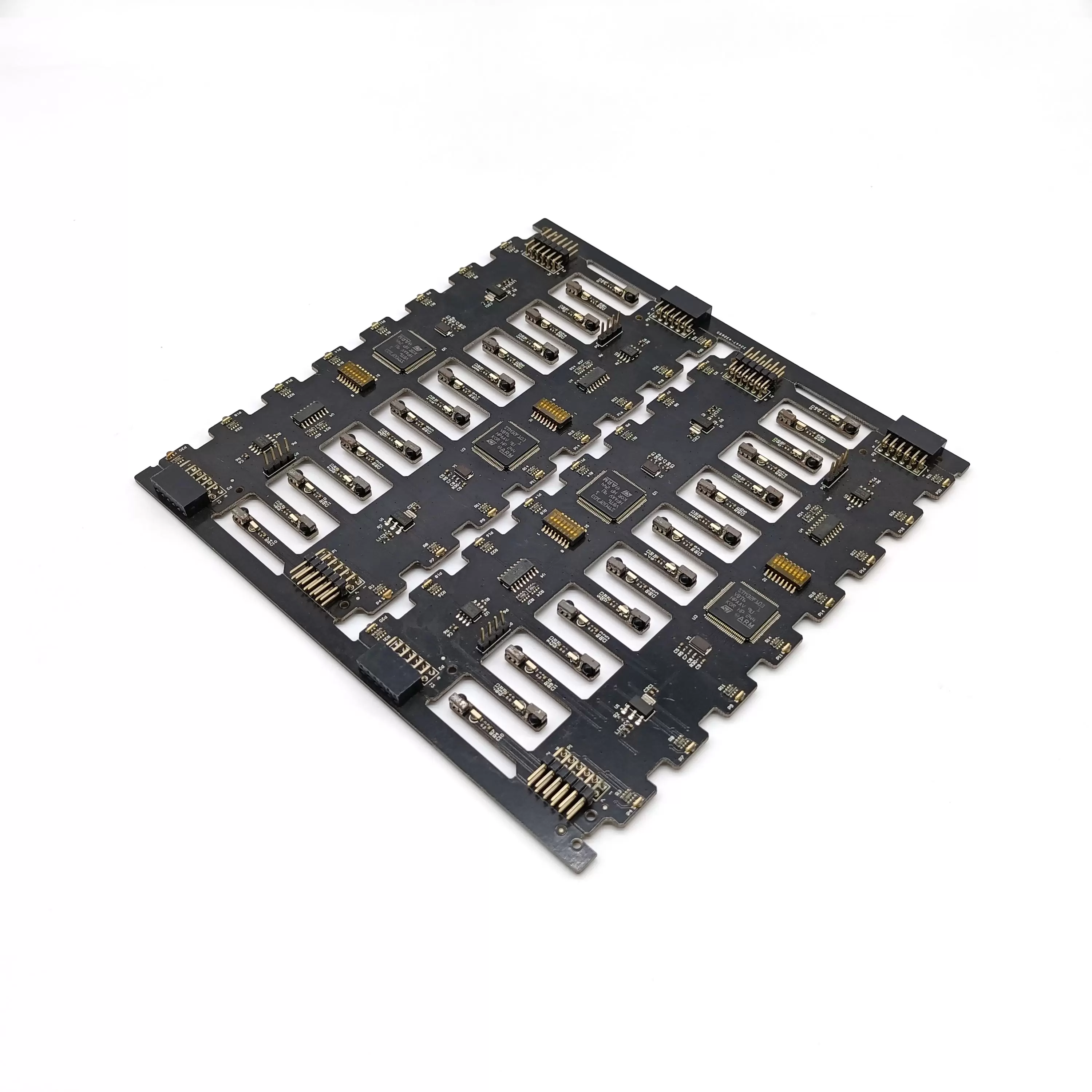
High-Density Component Placement
High-density component placement is essential for modern PCB assembly. This technique allows engineers to fit more features into smaller boards. Several methods make this possible:
●Surface Mount Technology (SMT) allows for higher component density and automated assembly.
●Micro-BGA enables ultra-small solder ball arrays for high pin-count ICs in compact spaces.
●3D PCB assembly maximizes functionality in constrained volumes, ideal for compact devices.
●Chip-On-Board (COB) reduces component height and improves signal integrity by directly bonding silicon dies.
●Ball-Grid Array (BGA) provides excellent thermal performance and connectivity for high-pin-count devices.
These methods help IoT devices deliver more functions without increasing their size. However, engineers face several challenges:
●Space constraints due to the need to fit advanced functionality into smaller sizes.
●Signal interference arising from tightly packed components.
●Thermal management challenges due to heat generated by components.
●Precise routing and component placement are required to maintain functionality and performance.
Engineers use automation and robotics to improve accuracy and speed during assembly. Automated optical inspection systems also help maintain quality. As miniaturization continues, careful planning and advanced techniques will remain vital for reliable device operation.
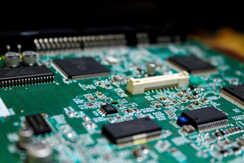
Signal Integrity and Power Management
PCB Assembly and Signal Integrity
PCB assembly for internet devices must protect signal integrity to ensure reliable connectivity. High-speed circuits require careful design, so signals travel accurately between components. Shorter traces help lower signal delay and prevent impedance mismatches. Grouped vias improve conductivity and reduce resistive losses, which enhances signal flow. Placing high-frequency signals on inner layers reduces delays and prevents signal bouncing. Power and ground planes on inner layers cut noise and crosstalk, providing a smoother signal path. Multi-layer boards increase complexity, but careful layout avoids interference from wireless modules. Engineers use advanced tools to simulate and optimize signal paths, especially as devices become smaller and more integrated.
Note: Excess reflection from connectors, inconsistent ground references, and incorrect trace entry can cause signal containment problems and radiation issues.
Low Power Operation
Many IoT devices depend on low-power operation to extend battery life. PCB assembly uses several methods to achieve this goal:
●Implementing sleep modes lets devices rest when not in use.
●Duty cycling controls when circuits are active, reducing energy waste.
●Choosing proper components helps lengthen battery life.
Power management ICs optimize voltage levels for different parts of the board. Smart power paths and materials contribute to energy savings. The PCB ensures that sensors, chips, and radios receive the right amount of energy, improving battery life on a single charge.
Power Management Feature | Description |
|---|
Power Management ICs (PMICs) | Provide tailored voltage levels, reducing energy waste. |
Smart Power Paths | Direct energy efficiently to components, saving power. |
Controlled Power Distribution | Ensures each module receives the correct energy, enhancing battery life. |
Stable Electrical Performance
Stable electrical performance is essential for networked devices. Via stitching enhances grounding and signal integrity, reducing electromagnetic interference. Low impedance paths in power distribution networks help maintain steady voltage. Decoupling capacitors near power pins filter high-frequency noise. High-quality materials, such as solder, ensure strong connections. Precision in component placement and soldering prevents short circuits and other issues.
Evidence Description | Role in Electrical Performance |
|---|
Interconnects act as 'glue + highways.' | Support stable performance and long-term reliability in PCB assemblies for internet connectivity. |
High-quality interconnects ensure consistent conductivity | Avoid resistance buildup, signal disruption, and localized overheating. |
Durable interconnects reduce rework | Extend product lifecycle and ensure reliable electronic assemblies for internet applications. |
PCB assembly supports stable operation by maintaining clear signal paths, managing power efficiently, and using quality materials. These practices help wireless devices deliver consistent performance in real-world conditions.
Quality and Reliability
Consistency Across Deployment
Consistency is a key factor in the success of PCB assembly for internet applications. When manufacturers produce thousands of IoT devices, each unit must perform the same way in the field. Small differences in solder joints, component placement, or thermal management can affect battery life and long-term stability. Reliable assembly processes help maintain uniformity across all devices.
Evidence Description | Impact on IoT Devices |
|---|
Variations in solder joints, component placement, and thermal management affect power consumption and long-term performance in deployed environments. | Consistent assembly ensures optimal battery life and device stability, crucial for IoT applications. |
Reliability is engineered into the manufacturing flow through conformal coating and thermal cycling tests. | Enhances device performance and reliability in diverse environments, essential for large-scale deployment. |
Design choices consider ease of assembly, testing, and mass production. | Facilitates scalability and cost-effectiveness in manufacturing for large-scale IoT device deployment. |
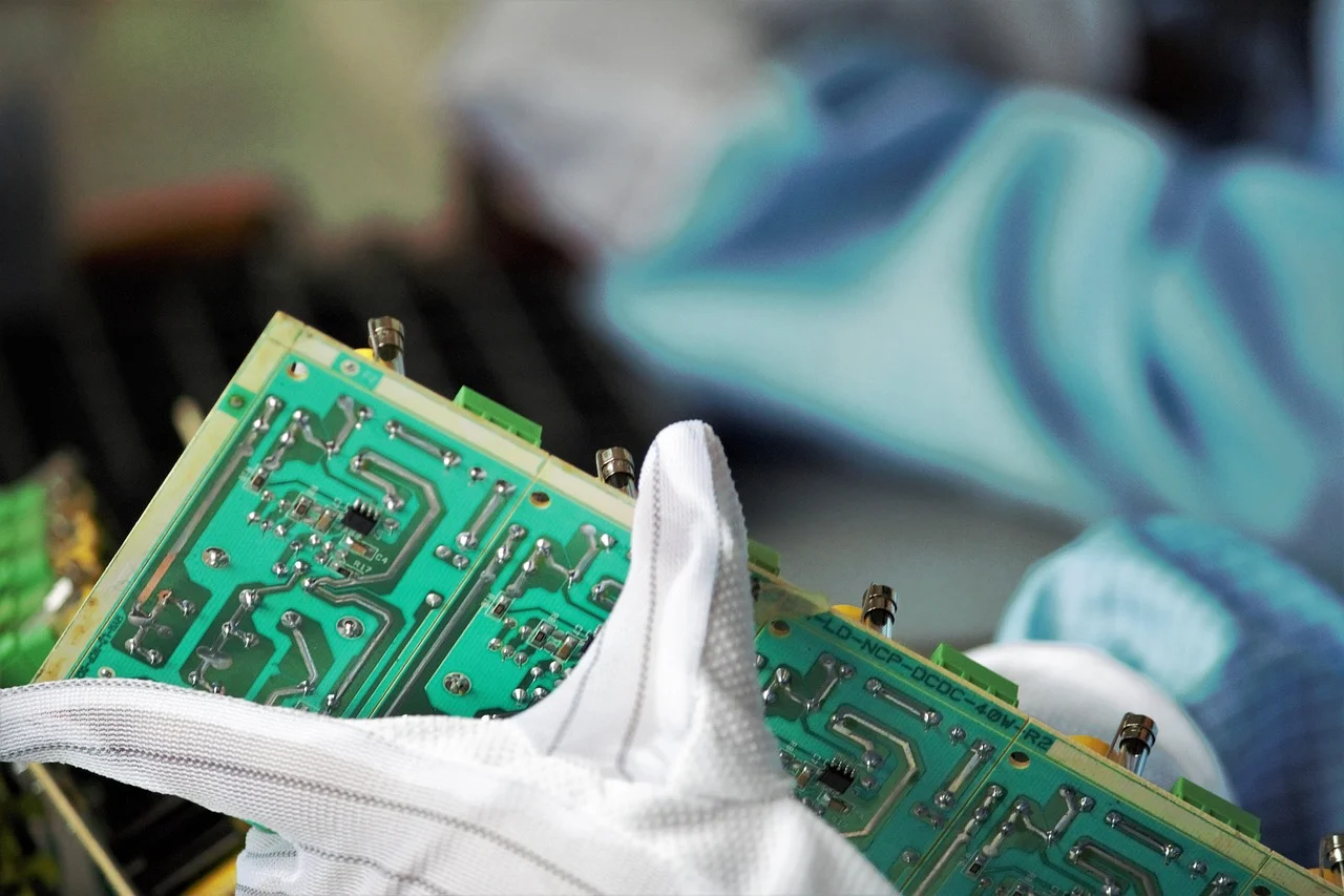
Testing and Inspection
Testing and inspection are essential steps in the PCB assembly process. Modern factories use advanced inspection technologies to detect defects early. Automated Optical Inspection (AOI) checks for missing components and solder issues. X-Ray Inspection reveals hidden problems inside solder joints. In-Circuit Testing (ICT) validates electrical connections, while Functional Testing (FCT) confirms that the board works as intended.
Testing Method | Description | Application |
|---|
In-Circuit Testing (ICT) | Validates components and checks for shorts/opens | Used in medium to high volume production |
Functional Testing (FCT) | Tests the board under actual operating conditions | Conducted at the final validation stage |
●Solder Paste Inspection (SPI) verifies the correct amount of solder paste.
●AOI checks placement and solder-joint quality.
●ICT tests electrical connectivity.
●Functional Test assesses end-use performance.
Incorporating Design for Testability (DFT) allows engineers to spot potential issues early, reducing production costs. Rigorous testing methods, such as AOI and ICT, help catch defects before devices reach customers. This approach ensures that PCB assembly delivers reliable performance for internet-connected products.
Challenges and Innovations
Scalability in PCB Assembly
Manufacturers face several challenges when scaling PCB assembly for internet-connected products. The complexity of modern boards increases as devices become smaller and more integrated. Engineers must fit multiple communication modules, sensors, and power management circuits onto a single board. This process requires precise placement and soldering to avoid signal interference and ensure reliable operation.
Regulatory compliance adds another layer of difficulty. Each region may have different standards for safety, electromagnetic compatibility, and environmental impact. Manufacturers must test and certify their products to meet these requirements. Consistent quality across large batches is essential. Automated inspection systems help detect defects early, but maintaining uniformity remains a demanding task.
A table below summarizes key challenges:
Challenge | Impact on Production |
|---|
Increased complexity | Requires advanced assembly techniques |
Regulatory compliance | Demands rigorous testing and certification |
Quality consistency | Essential for large-scale deployment |
Emerging Technologies
Innovations in PCB assembly are transforming the reliability and performance of IoT devices. Miniaturization allows engineers to create smaller boards for compact products. Advanced functionalities are now embedded within PCB layers, improving performance and reducing size. Sustainability efforts focus on eco-friendly materials and optimized processes to minimize environmental impact.
Automation and AI streamline production, improving efficiency and quality control. Flexible and rigid-flex PCBs enable new designs for wearables and medical devices. These layouts eliminate bulky wire harnesses and connectors, reducing size and weight. Fewer connectors and solder joints mean fewer points of failure, which increases reliability and extends operational lifespans.
HDI PCBs endure mechanical stress and thermal cycling, maintaining consistent performance even in demanding environments. Their multi-layer construction distributes stress evenly, preventing cracks or delamination. In automotive systems, HDI boards withstand vibrations and temperature swings, ensuring safety features work reliably.
PCB assembly forms the foundation for reliable internet connectivity in IoT and networked devices. High-speed communication, efficient power management, and robust assembly processes ensure devices work well in many environments.
Key Aspect | Description |
|---|
High-Speed Communication | Enables real-time data transfer in connected devices. |
Efficient Power Management | Extends battery life and reduces energy use. |
Reliability in Harsh Conditions | Maintains performance despite environmental challenges. |
Well-assembled PCBs power everyday products, from smartphones and medical devices to smart cars. As technology advances, innovations like miniaturization, flexible materials, and AI-driven manufacturing will continue to improve internet connectivity for everyone.
About the author:

Sonic Yang
As a major in Electronics and Mechanical Automation, Sonic has been engaged in PCB design, R&D, and manufacturing of electronics for around 22 years, as the engineering director, and coordinates with the supply chain(components and CNC parts), providing professional support and consulting for global customers.
 en
en

 WhatsApp