PCB castellated holes technology, also known as half-holes, edge-mounted metallized half-holes, or stamp holes (in some scenarios), is a special printed circuit board (PCB) processing technique. It is primarily used in modular design and direct board-to-board soldering connections, especially when a small PCB module (such as a Wi-Fi or Bluetooth module) needs to be soldered onto the motherboard like a surface-mount component.

1. Core Definition and Appearance
● Process Essence: On the edge of the PCB board, half of the plated through-hole (PTH) is precisely milled away along it's axis, forming a series of semi-circular, metallized openings.
● Visual Characteristics: A row of "U-shaped" or "C-shaped" metallized pads can be seen on the edge of PCB board, resembling the crenellations of a castle, hence the name "Castellated Holes."
2. Main Manufacturing Process
● Conventional PCB Fabrication: First, complete through-holes are manufactured on double-sided or multi-layer PCB board. These through-holes are located on the edge of PCB where the board will be separated in the future process, and the holes have already been metallized (electroplated copper, etc.).
● Milling/Rolling: Using a high-precision CNC milling machine (routing machine), the board edge area containing these through-holes is precisely milled away along a pre-designed path. The cutting path passes exactly through the center of each through-hole, dividing it in two.
● Post-processing: The cut surface is cleaned and deburred as possible to ensure that the metallization layer inside the half-hole is intact, smooth, and has good solderability.

3. Key Design Considerations
● Hole Diameter and Location: Through-holes with a diameter of 0.6mm to 1.0mm are typically used. The hole center must be precisely located on the board edge contour line.
● Pad Ring Width: The copper ring (pad) around the half-hole needs to be of sufficient width (usually ≥0.25mm) to ensure mechanical strength and soldering reliability, and to prevent the metallization layer from peeling off during cutting or soldering.
● Spacing: The spacing between half-holes needs to consider the PCB manufacturer's processing capabilities and the need to prevent bridging during soldering.
4. Key Advantages
● Space and Height: Eliminating the need for traditional sockets, connectors, or solder headers, enables board-to-board(even like PoP) surface mount technology (SMT), significantly reducing the overall module height and package.
● Simplify Assembly: Automated soldering can be performed directly using SMT and reflow soldering processes, improve production efficiency and reduce labor costs.
● Enhance Reliability: Direct and robust solder joints which avoid potential issues like poor contact or loosening up that might occur with connectors.
● Reduce Costs: Eliminates the cost and installation steps of additional connectors.
● Easy Testing and Replacement: Modules can be manufactured and tested independently before being soldered onto the mainboard/PCB. Even disassembly is not easy after soldering, but replace as a complete module is still relatively convenient.
5. Common Application Scenarios
● Standard Modules: Such as wireless communication modules (Wi-Fi, BLE, LoRa), sensor modules, power modules, etc., facilitating direct integration by customers.
● Motherboard/Daughterboard Structure: Such as the connection between the Arduino board (Shield) and the core board & baseboard.
● Space-constrained devices: Products with requirements for thickness, such as smartwatches, headphones, and portable medical devices.
● Transitional testing or adaptation design.
6. Difference from "Stamp-off Tabs"
● Castellated Holes: Specifically refers to metallized holes that are cut open for electrical connections and physical soldering.
● Stamp-off Tabs: Typically a series of non-metallized small holes or V-grooves, primarily for facilitating panel separation. Sometimes they can also serve as simple mechanical fixings or grounding, but are not used for primary electrical signal connections. Both may coexist on a single board.
7. Manufacturing Challenges
● Requirements for high precision : Milling precision directly affects the shape of the Castellated Hole/half-hole and the integrity of the metallization layer.
● Quality of Layer Metallization: After cutting, the copper layer at the castellated holes cross-section must be intact, without delamination or burrs; otherwise, soldering and reliability will be affected.
● Cost: More processing steps and higher process requirements than regular PCBs, therefore the cost is relatively higher.
In summary:
PCB castellated holes technology is a precise and efficient solution for surface mount connections on modular PCBs. It plays a crucial role in the miniaturization and modular design of modern electronic devices, balancing space, cost and reliability.
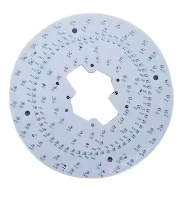
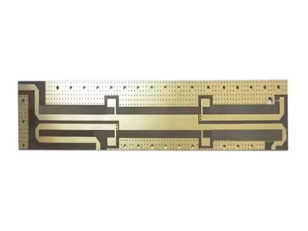
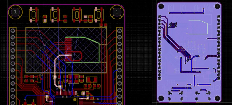
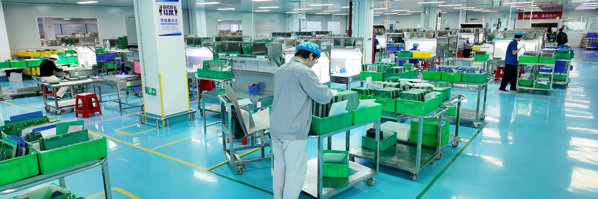
PCB manufacturing is Benlida's traditional main business and the start of career. For over 14 years, Benlida has keep investing modern advanced equipment, established a professional team, insist on quality first and customer-oriented service, committed to providing top-class PCB and PCBA manufacturing services to global customers!

About the auther:

Sonic Yang
As a major of Electronics and Mechanical Automation, Sonic has been engaged in PCB design, R&D, manufacturing of eletronics for around 22 years, as engineering director and coordinates with supply chain(components&CNC parts), providing professional supports and consults for global customers.
 en
en


 WhatsApp