A Comprehensive Guide for Component Inspection: From IQC Technician, Equipments to Standards, Comprehensive Incoming Quality Control
Electronic components are the fundamental elements of electronic products, their quality directly determines the reliability, lifespan, and even safety. Appearance inspection is the first and crucial step in quality control.
I. Focus on Appearance: What to inspect as IQC?
Appearance inspection focuses on the core information of components, surface defects and physical damages, includes:
1. Packaging/Marking Issues
- Marking Errors: Unclear, incorrect, or missing information such as model&part number, specification, D/C, batch info, or polarity markings.
- Packaging Defects: Damage, cracks, gaps, burrs, bubbles, stains, or discoloration of the package.
2. Pin/Lead Issues
- Oxidation/Contamination: Blackening, discoloration, or contamination on the pin&lead surface.
- Deformation/Damage: Bending, skewing, warping, detachment, or mechanical damage to pins.
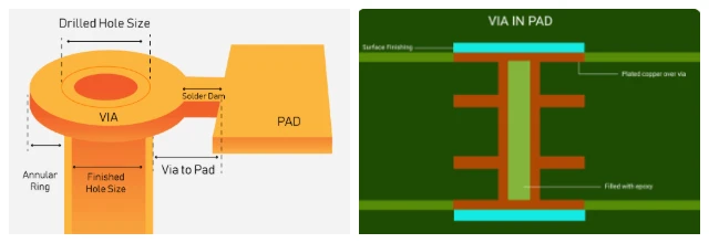
- Poor Coplanarity: Especially for multi-pin devices (such as QFPs), pin ends are not on the same plane, leading to poor soldering.
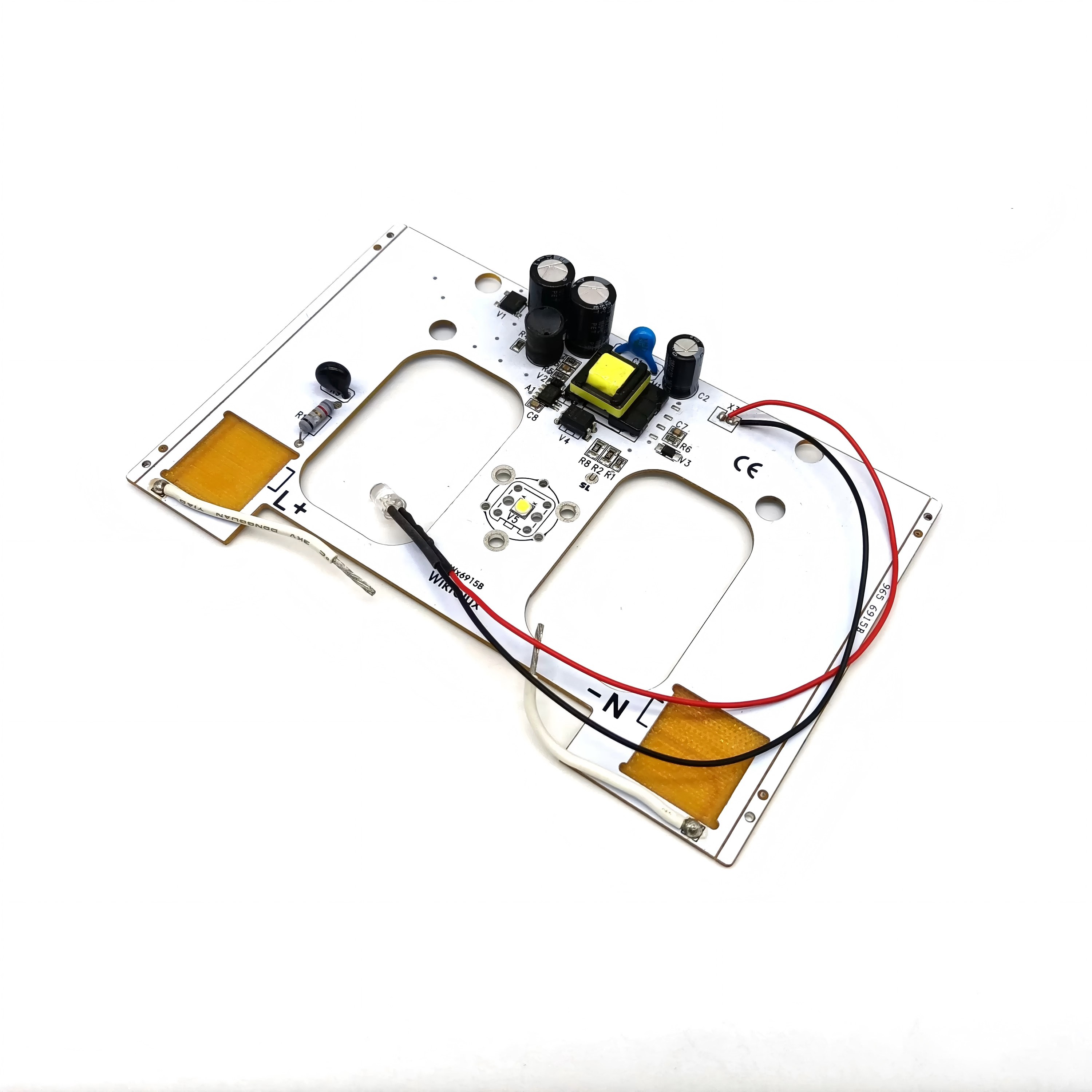
3. Solder Joint/Electroplation Issues
- Poor Plating: Uneven tin or silver plating, peeling, exposed copper, or corrosion.
- Pad Oxidation: For surface-mount components (such as capacitors and resistors), solder joint oxidation leads to poor solderability.
II. Inspection Methods: How to Inspect?
Currently, there are three methods commonly used, highly suitable for different scenarios:
1. Manual Visual Inspection
● Method: Under sufficient lighting, quality technicians observe the components by magnifying glass or microscope.
● Advantages: Flexible, low cost, suitable for small batches, multiple varieties, or exceptionally complex defect identification.
● Disadvantages: Low efficiency, prone to fatigue, highly subjective, inconsistent standards, and prone to missed defects.
2. Automated Optical Inspection(AOI)
● Method: On AOI equipment, high-resolution cameras capture images of components automatically, then compared with pre-set standard images to identify defects.
● Advantages: High speed, high efficiency, high accuracy, suitable for large-scale production.
● Disadvantages: High initial investment cost, requires skilled programmers and standard setting technicians, and may send false alarms.
3. X-ray Inspection
● Method: For hidden, covered defects (such as solder ball voids under BGAs, broken internal leads, and internal chip structures), AOI and the human eye cannot penetrate them, this situation requires X-ray inspection.
● Advantages: Non-destructive testing, capable to detect the internal issues and defects.
● Disadvantages: Expensive equipment, high daily maintenance costs, requires separate space, slow inspection speed, and employees might be reluctant to operate.
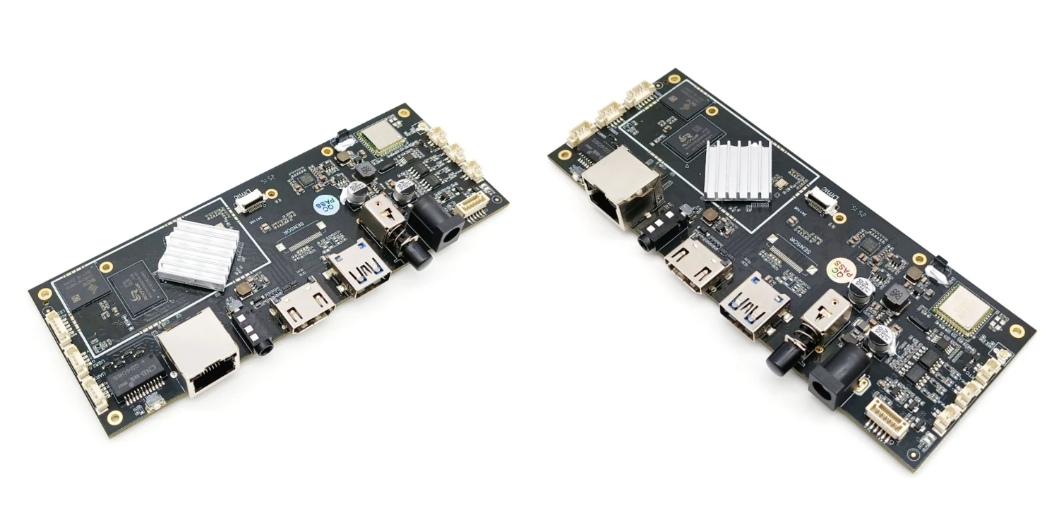
Benlida is professional to produce PCBs and PCBA, it has a dedicated quality team to inspect the components, ensuring the quality of components since first beginning of every PCBA:
1. Professional quality engineers and well trained technicians;
2. Professional AOI and X-Ray equipment, inspect efficiently and in-depth;
3. Collaboration with authoritative third-party organization, for technical support and professional reports to verify liability;
4. Professional verifications service: when there are risks of components, such as refurbished or counterfeit;
Benlida provides service for component inspection and reliability analysis:
1. Professional Inspection Equipment:
● High-magnification electron microscope: Precisely observes micron-level defects, such as microcracks and plating flaws.
● Automated optical inspection system: Efficiently performs initial screening of large batches of components, ensuring objectivity and consistency.
● High-resolution X-Ray inspection system: Non-destructively visualizes the internal structure of components, identifying refurbished parts (such as internal rewiring), counterfeit parts (such as internal chip sizes not matching markings), voids, and other defects.
2. Authoritative Standards and Reference
Strictly follow to international and domestic standards such as IPC-A-610 (Acceptability of Electronic Components) and JESD22 (Reliability Testing Methods for Solid State Devices), or inspect&assess by according to your company's standards&requirements, ensuring the impartiality and authority of the test results.
3. Added Value: From Appearance to Internal Structure
Inspection for appearance is only the first step. Benlida's inspection services include:
● Incoming Inspection: Safeguard the quality from supply chain and prevent defective component flow into production progress.
● Authentic Verification: Identifying refurbished and counterfeit components accurately, protecting your products and brand.
● Failure Analysis: When batch failures occur, by combining appearance inspection with electrical performance testing, open-shell analysis, and other methods, the root cause can be figured out—is it material issue, or from design and manufacturing process?
Choose Benlida, you choose:
1. Precision: Relying on professional equipment.
2. Efficiency: Automative equipment and professional team.
3. Authority: Issuing reliable reports based on industry standards.
4. Worry-free: One-stop production reduces your quality risks and management costs, while increasing production efficiency.
Benlida specializes in manufacturing high-quality PCB and PCBA, safeguarding the quality of your products and the value of your brand!
 en
en


 WhatsApp