PCB assembly brings electronic components together on a flat board called a PCB. This board acts as the foundation, allowing each part to communicate and work as a team. In the process, manufacturers place and solder components onto the PCB, making sure each piece stays secure and can transfer electricity. PCB assembly plays a vital role in modern electronics, especially in devices that rely on smart connections. For PCB Assembly for IoT Device, the PCB forms the backbone that enables sensors, processors, and wireless modules to function as one system.
Key Takeaways
●PCB assembly connects electronic components on a flat board, enabling devices to work together effectively.
●Engineers must carefully design and test PCBs to ensure reliability and performance in IoT devices.
●Quality control measures, like automated inspections, help catch defects early and improve device durability.
●Choosing the right components and assembly methods is crucial for creating compact and efficient IoT devices.
●Understanding common challenges in PCB assembly can help engineers avoid mistakes and enhance device functionality.
PCB Assembly Overview
Role in IoT Devices
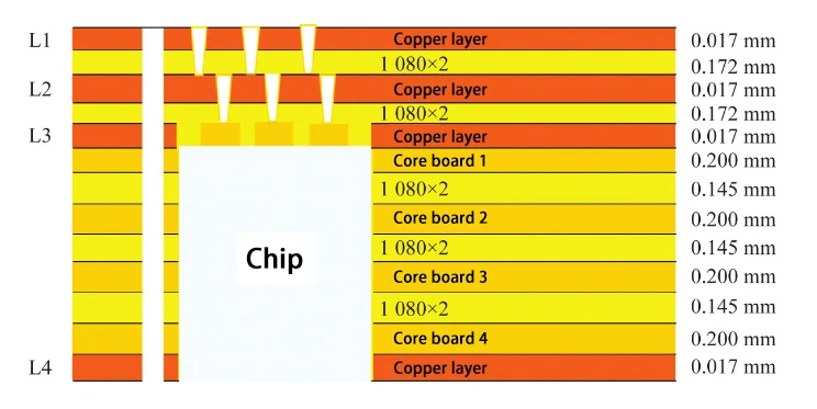
PCB assembly for IoT device manufacturing shapes the way modern technology connects and communicates. Engineers use PCB assembly to bring together sensors, processors, and wireless modules on a printed circuit board. This process allows devices to operate as a single unit. High-Density Interconnect technology lets designers fit more components into a smaller PCB, which is essential for compact IoT applications. Flexible PCB designs give mechanical flexibility, making them ideal for wearables and other devices that need to fit into tight spaces. Signal integrity improves with advanced PCB layouts, supporting reliable wireless communication. The backbone of IoT devices relies on PCB assembly to enable seamless integration and efficient data exchange.
Importance of PCB Assembly
PCB assembly stands at the core of reliable and scalable IoT solutions. The printed circuit board must support effective connectivity, power management, and quality control. Engineers use surface mount technology to place components closely, which allows for smaller yet functional devices. Careful PCB layout ensures controlled impedance traces, RF shielding, and antenna placement. These factors protect against electromagnetic interference and maintain ground plane continuity. Industrial IoT devices often face temperature extremes, moisture, vibration, and dust. Robust PCB assembly protects against these challenges and extends device lifespan.
●Seamless integration with other systems supports the overall architecture of IoT devices.
●Effective power management reduces heat and extends battery life.
●Quality control measures enhance reliability and durability.
●Scalable PCB assembly processes allow manufacturers to meet consumer demand quickly.
Design for Manufacture principles guide engineers to choose the right PCB materials and implement thorough testing. The backbone of IoT devices depends on PCB assembly to control performance and ensure connectivity. Without careful design and assembly, scalability issues can arise, limiting the success of IoT projects.
Step-by-Step Process for PCB Assembly for an IoT Device
The step-by-step process for PCB assembly for IoT devices ensures that every stage, from design to testing, supports the reliability and performance of smart devices. Each step addresses unique challenges in IoT applications, such as miniaturization, wireless connectivity, and power efficiency.
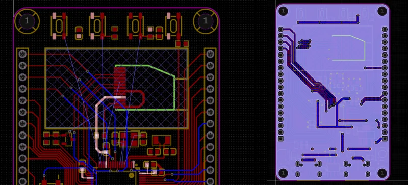
PCB Design and Prototyping
Engineers begin with PCB layout design, which forms the blueprint for the entire printed circuit board assembly. They select design software based on project needs. Popular tools include:
- Altium Designer, which offers advanced features for professionals.
- KiCad is a free, open-source option with strong community support.
- Eagle is known for its user-friendly interface.
- Online PCB design tools, which allow for easy collaboration.
During prototyping, engineers test the design in real-world conditions. They refine the layout to improve performance and durability. The cost and lead time for prototypes can vary. For example, a simple double-layer PCB prototype may cost between $100 and $300, while a complex multilayer version can reach $1,500. IoT device PCB prototypes usually range from $200 to $400 per unit, with standard lead times of 5-7 business days. Faster delivery increases costs, so teams must balance speed and budget.
Component Sourcing and Preparation
Component selection plays a critical role in PCB assembly for an IoT device. Engineers consider the application’s requirements, such as form factor, communication protocols, and power consumption. They choose compact, energy-efficient parts and plan their placement to minimize interference. Signal integrity and power management guide these decisions.
Supply chain resilience is essential. Global shortages, like the chip crisis in 2021, caused production delays for many manufacturers. Even one missing component can halt the entire process. Engineers now address sourcing challenges early in the design phase to avoid delays and maintain flexibility.
| Criteria | Description |
|---|
| Application Requirements | Understand specific needs, including form factor and protocols. |
| Component Selection | Choose compact, power-efficient parts and ensure proper placement. |
| Signal Integrity | Maintain signal quality through impedance matching and short trace lengths. |
| Power Management | Use low-power components and energy harvesting methods. |
| Environmental Factors | Design for humidity, temperature, and add protective coatings if needed. |
Cleaning and Inspection
Before assembly, technicians clean the PCB to remove contaminants. Cleanliness prevents defects and improves reliability. Industry standards guide this process:
| Standard | Description |
|---|
| IPC-5704 | Sets cleanliness requirements for bare PCBs before assembly. |
| IPC-A-610 | Defines cleanliness criteria for assembled PCBs, with three reliability classes. |
| IPC-J-STD-001 | Covers soldered assemblies, including post-soldering cleanliness and contamination limits. |
Inspection follows cleaning. Common techniques include Automated Optical Inspection (AOI), X-ray inspection, and manual visual checks. AOI compares actual component placement with design files. X-ray inspection reveals hidden defects. Manual inspection helps spot subtle issues that machines might miss.
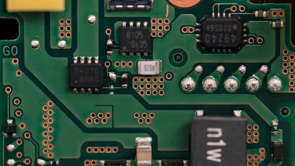
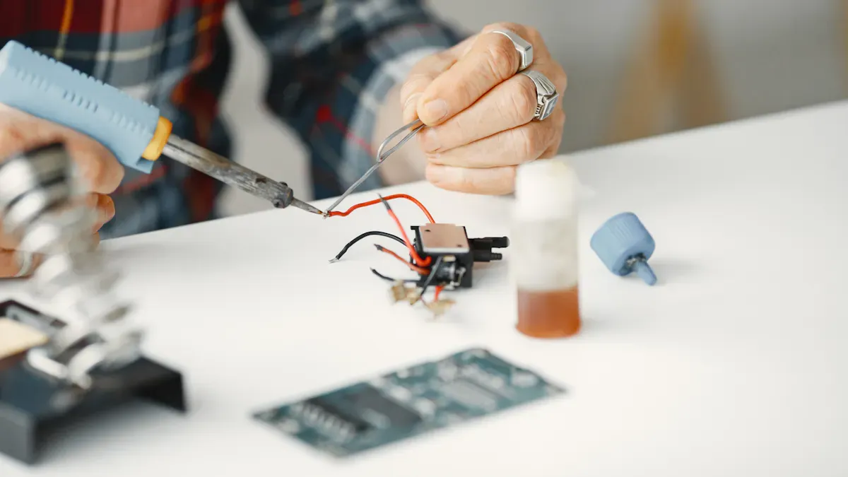
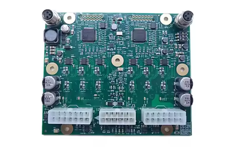
Component Placement and Soldering
Component placement and soldering form the heart of PCB assembly for IoT devices. Engineers use two main methods:
| Method | Description |
|---|
| Surface Mount Technology (SMT) | Dominates modern designs, ideal for high-density IoT boards with tiny components. |
| Through Hole Technology (THT) | Used for connectors and power components that need mechanical strength. |
| Reflow Soldering | Preferred for SMT; involves applying solder paste, placing components, and heating in a reflow oven. |
| Wave Soldering | Used for THT; the PCB passes over molten solder to create connections. |
Automated systems ensure uniform placement and soldering, which leads to lower defect rates. Manual soldering, while useful for prototypes, has higher error rates. Automated processes can achieve error rates as low as 0.01%. This reliability is vital for IoT devices that must operate without failure.
Wireless Module Integration
Wireless modules connect IoT devices to networks. The most common modules include Wi-Fi, Bluetooth, and LoRa. Wi-Fi modules appear in smart home appliances, industrial sensors, and wearables. They provide reliable, widespread connectivity for remote access and control.
Integrating wireless modules presents challenges. Engineers must fit many components into small spaces. They select materials that minimize RF transmission loss and manage heat from RF parts. Embedding sensors and modules in a limited space requires careful planning.
●Wi-Fi modules
●Bluetooth modules
●LoRa modules
These modules enable network connectivity in modern IoT devices.
Programming and Testing
Programming and testing complete the PCB assembly for the IoT device. Engineers add programming headers for firmware updates and test points for production checks. They may use boundary scan (JTAG) for complex boards and include configuration interfaces.
Testing includes several procedures:
| Procedure Type | Description |
|---|
| Prototyping | Test designs in real-world conditions and refine for performance and durability. |
| In-Circuit Testing (ICT) | Verify electrical connections on the PCB. |
| Functional Testing (FT) | Ensure the PCB performs as intended under operational conditions. |
| Environmental Stress Testing | Simulate real-world conditions to assess durability and reliability. |
Engineers use these tests to confirm that the printed circuit board works as designed. They check for electrical faults, functional errors, and durability under stress. This step ensures that the final devices meet quality standards and perform reliably in the field.
The step-by-step process for PCB assembly for an IoT device combines careful planning, precise execution, and thorough testing. Each stage supports the creation of reliable, high-performance devices that power the Internet of Things.
Common Challenges in PCB Assembly
Placement and Soldering Issues
Engineers face several obstacles during PCB assembly, especially when working with compact IoT designs. Miniaturization increases component density and requires precise placement. Common placement and soldering issues include insufficient solder, component misalignment, voids in solder joints, solder balling, lifted pads, wrong component placement, and PCB warpage. The table below outlines the main causes and prevention strategies for these problems:
| Issue | Causes | Prevention Strategies |
|---|
| Insufficient Solder | Blocked stencil, misalignment, paste drying | Clean stencils, monitor paste, and use automated systems |
| Component Misalignment | Calibration errors, vibrations, and warping | Calibrate machines, use vision alignment, and proper storage |
| Voids in Solder Joints | Outgassing, excess paste, contamination | Optimize paste, vacuum reflow, and clean surfaces |
| Solder Balling | Excess paste, high temperature, and moisture | Control paste volume, follow reflow profiles |
| Lifted Pads or Traces | High temperature, poor laminate, rework | Use quality laminates, proper rework, and avoid reheating |
| Wrong Placement | Human error, labeling, and lack of verification | AOI, barcode tracking, operator training |
| PCB Warpage | Excess heat, uneven cooling, poor storage | Use high-Tg materials, store flat, control gradients |
Wireless Connectivity Problems
Wireless connectivity presents unique challenges in PCB assembly for IoT applications. Engineers must integrate antennas directly onto the PCB, which complicates layout and signal integrity. Careful design of embedded antennas is essential. Placement and ground plane design affect performance. Multiple wireless technologies in one printed circuit board can cause electromagnetic interference. Managing EMI and ensuring electromagnetic compatibility requires advanced layout techniques and shielding.
●Integration of antennas onto the PCB increases layout complexity.
●Embedded antenna design depends on placement and ground plane.
●EMI and EMC issues arise when multiple wireless protocols coexist.
Testing and Troubleshooting
Testing and troubleshooting ensure that each PCB functions as intended. Engineers use several methods to resolve issues:
1. They maintain test probes and clean them regularly for accurate contact.
2. They check fixture alignment and inspect for wear.
3. They review the in-circuit test program settings and control environmental factors.
4. They improve component accessibility by following design-for-test principles.
5. They update software and calibrate systems to maintain testing accuracy.
Common challenges in PCB assembly for IoT devices include miniaturization, power management, thermal management, connectivity, EMI/EMC, and security. Addressing these challenges ensures reliable performance and long-term durability.
Best Practices for PCB Assembly
Quality Control Tips
Quality control ensures that every PCB meets high standards for reliability and performance. Technicians use several inspection and testing methods to catch defects early. Solder paste inspection checks the amount of solder before placing components. Automated optical inspection uses advanced imaging to verify component placement and solder joints. In-circuit tests confirm electrical connections, while functional tests assess how the PCB performs in real-world conditions. The table below summarizes these key quality control measures:
| Quality Control Measure | Description |
|---|
| Solder Paste Inspection (SPI) | Verifies solder paste volume before component placement to prevent defects. |
| Automated Optical Inspection (AOI) | Inspects for component placement and solder-joint quality using advanced imaging technology. |
| In-Circuit Test (ICT) | Test the electrical connectivity of components on the PCB. |
| Functional Test | Assesses the performance of the PCB in its intended application. |
Technicians also follow industry certifications to maintain best practices. Certifications like IPC, ISO, RoHS, UL Listing, and ITAR set standards for safety, quality, and environmental responsibility. These certifications help manufacturers deliver reliable printed circuit board assembly for critical applications.
| Certification | Description |
|---|
| IPC | Defines and classifies accepted industry practices for PCB assembly, widely adopted by OEMs and EMS providers. |
| ISO | Ensures rigorous quality management standards, improving communication, efficiency, and customer satisfaction. |
| RoHS | Aims to reduce hazardous materials in electronic equipment, promoting environmentally friendly alternatives. |
| UL Listing | Addresses safety requirements for PCB assembly, crucial for preventing fire and electrical shock risks. |
| ITAR | Protects sensitive technology from espionage, incorporating tamper-resistant features in PCB assembly. |
Reliable Assembly Methods
Engineers use proven assembly methods to minimize defects and improve efficiency in PCB assembly. Surface mount technology works well for high-density boards, providing strong connections through reflow soldering. Through-hole technology adds mechanical strength for components that face physical stress. Reflow soldering needs a precise thermal profile and a clean environment to avoid defects. Wave soldering works efficiently for through-hole components, focusing on proper flux application and solder temperature control. Automated optical inspection detects defects early and helps refine the assembly process.
●Surface Mount Technology (SMT): Ideal for high-density PCB, ensuring strong connections.
●Through Hole Technology (THT): Provides strength for stressed components, with precise hole sizing.
●Reflow Soldering: Needs accurate thermal control and cleanliness.
●Wave Soldering: Efficient for through-hole parts, with careful flux and temperature management.
●Automated Optical Inspection (AOI): Detects defects early and supports process improvement.
Engineers who follow these best practices create reliable PCBs for modern devices. Careful attention to quality and method selection leads to successful printed circuit board assembly and long-lasting performance.
The PCB assembly process for IoT devices involves design, sourcing, cleaning, assembly, integration, and testing. Each step supports device reliability and performance.
●Careful PCB design, assembly, and testing improve durability and uncover hidden defects.
●Field and live testing confirm that PCB devices meet real-world demands.
Engineers can explore resources on PCB assembly methods, design strategies, and industry trends. The table below lists recommended online courses for those interested in advancing their PCB knowledge.
| Course Title | Description | Link |
|---|
| PCB Fabrication Technology | Hands-on course on PCB manufacturing processes. | Link |
| High TG Rigid Flex PCB for IoT Devices | Specialized course for IoT device PCB design. | Link |
FAQ
What is the difference between PCB and PCB assembly?
A PCB is a bare board with copper traces. PCB assembly means placing and soldering electronic components onto the board. The assembly process creates a working circuit.
Why does PCB assembly matter for IoT devices?
PCB assembly connects sensors, processors, and wireless modules. This integration allows IoT devices to collect data, process information, and communicate wirelessly.
How do engineers test assembled PCBs?
Engineers use automated optical inspection, in-circuit testing, and functional testing. These methods help detect defects, verify connections, and ensure reliable performance.
What are common mistakes in PCB assembly?
●Using incorrect components
●Poor soldering techniques
●Skipping cleaning steps
●Ignoring design guidelines
These mistakes can cause device failure or reduce lifespan.
About the auther:

Sonic Yang
As a major of Electronics and Mechanical Automation, Sonic has been engaged in PCB design, R&D, manufacturing of eletronics for around 22 years, as engineering director and coordinates with supply chain(components&CNC parts), providing professional supports and consults for global customers.
 en
en


.jpg)
 WhatsApp