On the PCB(Printed Circuit Board), solder mask plays a critical role: protecting PCB copper by against oxidation and corrosion, and solder mask dam is a dam-like element between 2 solder pads: solder mask material is incompatible with solder paste, thus the dam could create a separation and isolate solder paste on adjacent pads during soldering, by surface tension, preventing solder bridging and short circuits, also frame the solder paste during reflow&wave soldering process, assisting the alignment of components. (To avoid assembly failure like photo below: bridged solder paste and shorted pins.)
")
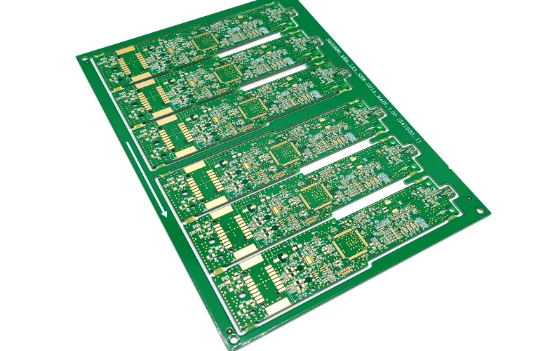
Solder mask dam normally processed by negative film output, where the no-opening area covered by solder mask material(ink) to form a physical isolation dam (while the opened area exposes the copper substrates for soldering). Design specifications require a standard width ≥ 6 mil (0.152 mm). It's size is directly related to the IC pad spacing, for example, an 8 mil pad spacing requires a 2 mil opening allowance on each side to maintain the solder mask dam. This technology is widely used in high-precision component mounting, such as BGA, MCU/chips, and components package 01005, and particularly effective when soldering IC pins with a pitch of less than 0.35mm.
The minimum width of the solder mask dam varies with the copper thickness of the substrate: for 1OZ copper substrate, if applying green solder mask ink, the minimum width is 0.1mm(4 mil), and other colors of solder mask ink require ≥ 5 mil. Standard designs require a distance of at least 0.2mm between solder pads. For multilayer boards, the solder mask openings and solder pads must be strictly designed to be the same dimension, while for single-layer boards, engineering compensation ensures the accuracy of dam width. For thicker copper substrates (2-4OZ), the width of the glossy black ink needs to be increased to ≥6 mil for tolerance amendments.
Statistics shown that package QFP without solder mask dam have higher short-circuit rate as 23%, after wave soldering, compared to boards with dams. Furthermore, the solder mask dam could reduce difficulty and avoids damage during repair work.
There is a certain relationship between solder mask dam's height, width and pad spacing. Below are common design rules:
1) The height of the dam is determined by the thickness of solder mask, normally 0.01-0.05mm;
2) The width of the dam is depending on the pads, for example:
● When the IC pad spacing is 8mil, a 2mil single-sided opening shall retain width as ≥0.1mm(approximately 4mil);
● The pad spacing for through-hole components needs to be ≥0.2mm (approximately 8mil);
3) The width of solder mask dam, on large copper areas needs to be ≥8mil to prevent short circuits during wave soldering;
Green ink, due to its highest process maturity, allows for more precise control of the width of solder mask dam. Statistics shown that under the same substrate conditions, compare to white ink, green ink could reduce the minimum retention width by 20%. And for black ink, due to harder to control during processing, it requires an amendment 1-2mil for solder mask dam width in practical applications.
PCB industry applies software for solder mask dam analysis, which identifies solder mask dam areas below 4mil in PCB design and could automatically provide optimization suggestions. For extreme cases where dam width requirements cannot be met, engineering solutions include:
● Adopting a fully open solder mask design, but it raises the risk of short-circuit;
● Adjusting the pad spacing to ≥0.4mm to coordinate process capabilities;
● Replacing by a high-precision ink type (such as matte green solder mask) to improve the process capacity;
Shenzhen Benlida Circuits Co.,Ltd has been manufacturering for PCB for 14 years, we always prioritize quality as first doctrine and insist rigorous quality management. For solder mask dam, this process is well managed and proceed here in Benlida, rigorous process engineering review and supervision are conducted to ensure quality and prevent defects. If you need PCB, please feel free to contact Shenzhen Benlida Circuits Co.,Ltd. and it will be highly appreciated if you can share Gerber files with requirements as well.
 en
en

 WhatsApp