What is the plating process in PCB Manufacturing?
If you’re evaluating a PCB Fabrication Service, it helps to understand why plating is one of the most important steps behind PCB reliability. PCB plating is not just “metal deposition”—it's the process that turns drilled holes and copper features into durable electrical interconnects that survive assembly heat, vibration, and long-term field use. In this guide, we’ll narrate and explain the full PCB plating process, what happens before and after plating, how copper plating differs from surface finishing, and how to choose the right finish for your end application.
1. PCB Plating Explained in Plain Language
PCB plating is the controlled formation of metal layers—primarily copper—on the board surface and inside drilled holes so the PCB traces can carry current, connect layers, and support soldering reliably.
What PCB plating actually does (beyond “metal deposition”)
Plating does three practical jobs:
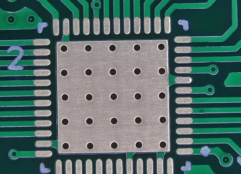
Creates electrical connections between layers by metallizing hole walls (vias and through-holes).
Builds mechanical strength in vias and pads by adding copper thickness where stress concentrates.
Prepares the PCB for assembly by ensuring the board is solderable and resistant to oxidation.
Copper plating vs surface finishing (don’t mix these up)
Copper plating builds structural copper—especially inside holes and on traces.
Surface finishing (ENIG, HASL, OSP, etc.) is the final protective/solderable coat on exposed copper pads.
They hold the roles for each function and cannot be replaced by each other.
Why plating is mandatory in modern PCB manufacturing
Without plating, multilayer PCBs would have no reliable way to connect internal layers, and even simple boards would suffer from rapid copper oxidation, poor soldering, and weak pad durability. In short: plating is what turns a patterned copper board into a functional circuit board.
2. Why PCB Plating Is Critical to PCB Reliability
Plating directly affects the connection between PCB layers:
Electrical conduction between layers
Vias are not “holes”—they are conductive but holes are not. Plating forms that conduction and ensures stable conduction between layers.
Mechanical reinforcement of vias and pads
A via with insufficient copper thickness might fail under heat cycling. Plating adds the copper on “structure” that support the via intact.
Impact on solderability and assembly yield
Sometimes solder defects could be traced back to surface condition. A properly controlled plating + finish system improves wetting, reduces rework, and stabilizes quality across lots.
3. Where PCB Plating Fits in the PCB Manufacturing Process
A simplified flow looks like this:
Drilling → Desmear → Activation → Plating → Imaging → Etching → Surface Finish
Why plating bridges mechanical drilling and electrical performance
Drilling creates a mechanical feature. Plating turns it into an electrical interconnect. That’s why drilling and plating are inseparable in reliability planning.
4. Two Cores of PCB Copper Plating Processes
Copper plating is the foundation. Everything else builds on it.
4.1 Electroless Copper Plating (Chemical Copper)
After drilling, hole walls are non-conductive (epoxy/glass). Electroless copper deposits a thin, continuous conductive layer so the hole can later be electroplated.
Key points:
● Why it’s needed: electroplating requires conductivity; raw hole walls don’t have it.
● Principle: an autocatalytic chemical reaction deposits copper evenly on activated surfaces.
● Purpose: create a continuous seed layer for reliable via formation.
● Reliability role: a poor electroless layer can lead to voids, skips, or weak adhesion later.
4.2 Electrolytic Copper Plating (Electroplating)
Once a conductive seed exists, electroplating builds copper thickness using controlled current.
Key points:
● How it works: electrical current drives copper ions to deposit on conductive surfaces.
● Via strengthening: builds copper thickness on the hole wall (barrel) and surface copper.
● Thickness control: managed by current density, bath chemistry, agitation, and time.
Why it can’t replace electroless copper: electroplating cannot start reliably on non-conductive hole walls.
5. PCB Plating Pretreatment Steps (Often Ignored, Highly Important)
Plating quality is decided before plating starts. Pre-treatment is where many failures are planted.
Deburring and desmear
Drilling leaves resin smear and debris. If not removed, copper cannot bond properly to the hole wall.
Alkaline degreasing
Removes oils and residues from prior processes. Contamination will hurt adhesion and increases void risk.
Micro-etching
Creates a controlled surface texture that improves copper adhesion and consistency.
Activation (palladium or alternative catalysts)
Activation seeds catalytic sites for electroless deposition. Poor activation can cause discontinuities and weak via barrels.
Why poor pretreatment causes delamination and voids
If the copper seed layer isn’t well-adhered or continuous, later electroplating amplifies the problem—resulting in voids, thin spots, and reliability failures.
6. Types of PCB Plating Methods (Use-Case Driven)
6.1 Through-Hole Plating (PTH)
The most common plating function in multilayer PCBs:
● forms conductive barrels in holes
● enables electrical interconnection between layers
● requires consideration of hole aspect ratio for uniform copper deposition
6.2 Selective / Brush Plating
Used for:
● local reinforcement
● repair/rework scenarios
● low-volume adjustments where full replating isn’t feasible
6.3 Finger Plating (Hard Gold Plating)
For edge connectors:
● excellent wear resistance
● low contact resistance
● stable mating performance for repeated insertion cycles
6.4 Reel-to-Reel Selective Plating
Often used in connector and leadframe-like applications:
● high throughput
● automated, consistent selective deposition
● efficient for mass production of plated contact regions
7. PCB Surface Finishes vs. PCB Copper Plating (Clear Distinction)
Many engineers whom are not familiar with fabrication, might mix up PCB copper plating with surface finishing. They’re related, but they reach different targets—and they are different stages of the PCB plating process.
Copper plating = building the conductive “structure”
Copper plating is the structural layer of the PCB. It forms:
● Via barrels and plated through-holes so layers are electrically connected
● Copper thickness on traces/pads to meet current, thermal, and reliability requirements
Think of copper plating as the part that makes the board electrically complete and mechanically strong.
Surface finish = protecting copper and enabling soldering
A surface finish is the final protective and solderable surface applied to exposed copper pads (and sometimes traces). It exists after copper plating because:
● copper oxidizes quickly in humid environment, which hurts solder wetting and increases resistance
● assembly needs controlled, repeatable solderability (especially for fine-pitch parts)
● some applications require special contact behavior (e.g., edge connectors needing hard gold)
The common misunderstanding (clarified)
A surface finish does not replace copper plating. Finishes like ENIG, HASL, OSP, immersion silver/tin are typically very thin and mainly serve for solderability/corrosion protection. Copper plating is what ensures layer-to-layer continuity and via reliability. In short:
● Copper plating = connectivity + strength
● Surface finish = solderability + protection
8. Common PCB Surface Finishes and Their Trade-Offs
8.1 HASL / Lead-Free HASL
● Strength: cost-effective, widely used
● Limit: planarity can be less ideal for very fine pitch
8.2 ENIG
● Strength: flat surface, good corrosion resistance, fine-pitch friendly
● Consideration: process control is critical to avoid issues like black pad
8.3 Immersion Silver
● Strength: good electrical performance for certain high-frequency needs
● Risk: more sensitive to handling and storage conditions
8.4 Other finishes (quick comparison)
● OSP: cost-effective for SMT, but storage/handling control is important
● Immersion tin: solderability-focused, requires storage discipline
● ENEPIG: good for advanced assembly needs (fine pitch, wire bonding scenarios)
● Hard gold: best for wear contacts (edge fingers), higher cost
9. Key Technical Parameters That Define Plating Quality
Copper thickness (vias vs surface)
A strong PCB needs proper copper where stress is highest—often in via barrels and pads.
Aspect ratio limits
High aspect ratio holes are harder to plate uniformly. The risk is thin copper in the center of the barrel.
Current distribution
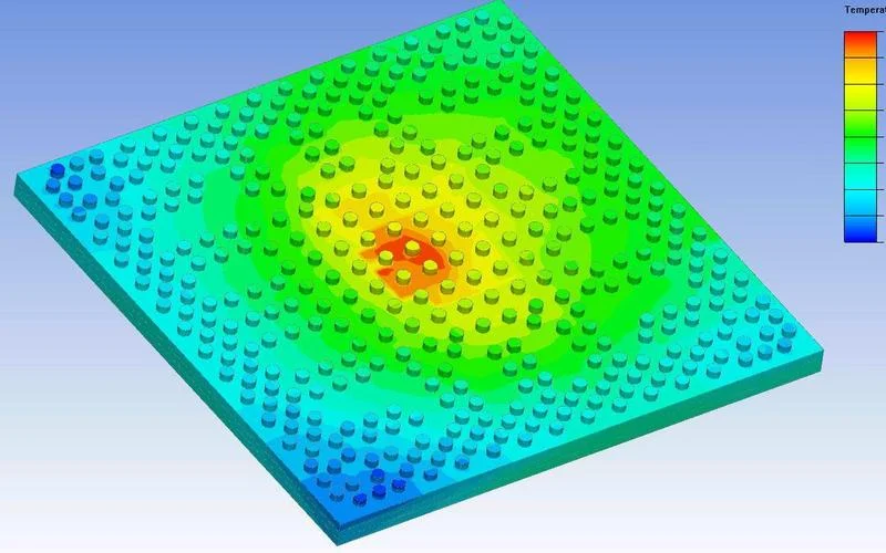
Current doesn’t distribute evenly across complex panels unless the process is tuned. Poor distribution causes uneven thickness.
Uniformity and throwing power
“Throwing power” describes how well plating reaches deep into holes. Better throwing power improves via reliability.
Adhesion strength
Adhesion is affected by pretreatment, micro-etch control, activation, and bath stability. Weak adhesion can lead to barrel cracks and delamination.
10. Common PCB Plating Defects and Root Causes
Void formation
Often caused by:
● poor desmear/cleaning
● incomplete activation
● trapped air or chemistry issues during deposition
Thin via copper
Can result from:
● challenging aspect ratios
● inadequate throwing power
● poor current distribution or time control
Delamination
Typically linked to:
● contamination
● poor adhesion due to pretreatment gaps
● material compatibility issues under thermal stress
Black pad (ENIG-related)
A surface finish defect tied to nickel/gold process control. It’s not “copper plating,” but it’s part of the finishing system that affects solder reliability.
Uneven copper buildup
Usually caused by:
● current crowding
● panel density effects
● inadequate process optimization for mixed feature distribution
11. Advanced and Modern PCB Plating Technologies
Pulse electroplating
Uses controlled pulse current to improve deposit structure, potentially helping uniformity in demanding features.
Vertical continuous plating (VCP)
Improves consistency and throughput for certain production profiles through controlled flow and uniform deposition conditions.
Direct metallization (palladium-free)
Alternative approaches that reduce dependency on traditional palladium activation systems and can simplify process control in some lines.
HDI and microvia plating challenges
Introduction for Microvias:
● smaller diameters
● different geometry (depth/diameter)
● higher sensitivity to voids
Process tuning becomes critical to maintain reliable via fill and consistent copper thickness.
12. Design Tips to Optimize PCB Plating Cost and Yield
Via size and aspect ratio optimization
Design vias that are plateable reliably. Extreme aspect ratios increase defect risk and cost.
Avoid unnecessary copper thickness
Over-specifying thickness increases time and risk without improving performance in many designs.
Copper balance strategies
Balanced copper distribution improves:
● plating uniformity
● reduced warpage risk
● consistent thickness across panels
Designing for manufacturable finishes
Choose a finish that matches:
● component pitch and assembly method
● shelf life needs
● environment (humidity, corrosion, wear contacts)
13. How to Choose the Right PCB Plating and Surface Finish
Choosing the right PCB plating approach and surface finish isn’t about picking the “best” option—it’s about matching reliability needs, assembly risk, and total cost. Below is a buyer-friendly way to decide, without getting lost.
Step 1: Start with the application environment
Ask what the board must survive:
● High humidity / corrosive atmosphere: prioritize finishes with stronger corrosion resistance and stable storage behavior.
● High temperature cycling / vibration: focus on via plating robustness (uniform copper thickness, strong adhesion) because mechanical stress shows up first in vias and pads.
● Wear/contact applications (edge connectors): plan for hard gold finger plating rather than standard solderable finishes.
Step 2: Match the finish to your assembly method
Assembly requirements often narrow the choice quickly:
● Fine-pitch SMT, BGA, dense layouts: you generally need a flat, consistent finish to reduce short and rework risk.
● General SMT / mixed technology: you have more flexibility, choose based on storage, cost, and process stability.
● Multiple reflow cycles or tight yield targets: prioritize finishes that maintain solderability through thermal exposure and handling.
Step 3: Define shelf life and logistics reality
How long will boards sit before assembly—and under what conditions?
● Long storage, international shipping, uncertain production windows: choose a finish with more forgiving shelf life and packaging tolerance.
● Fast turn builds with controlled storage: you can consider finishes that demand stricter handling, if they offer benefits for your design.
Step 4: Budget the right way (avoid “cheap becomes expensive”)
Instead of comparing unit price only, compare total cost of the whole production:
● scrap/rework risk
● inspection requirements
● field return risk
● schedule stability if a finish is more sensitive to handling
Practical decision matrix (engineers + buyers)
Your Priority | Plating Focus (Copper) | Finish Focus (Surface) | Why it matters |
Highest reliability / harsh use | Tight control of via copper thickness + adhesion | Corrosion-resistant, stable finish | Prevents barrel cracks, oxidation, field failures |
Fine-pitch, high-density assembly | Uniform plating + consistent pads | Flat finish compatible with fine pitch | Improves yield, reduces bridging/rework |
RF / high-speed performance | Consistency and uniformity (avoid discontinuities) | Finish with stable electrical behavior + controlled handling | Minimizes loss variation and assembly defects |
Cost-sensitive but stable production | Standard plating spec, good uniformity control | Practical, widely supported finish | Keeps cost down without risking yield |
Edge connectors / frequent mating | Reinforced copper where needed | Hard gold on fingers | Wear resistance + low contact resistance |
14. PCB Plating FAQs
1.Why is electroless copper plating necessary?
Because drilled hole walls are not conductive. Electroless copper creates the seed layer so electroplating can build thickness reliably.
2.How thick should via copper be?
It depends on reliability class, aspect ratio, and application stress (thermal cycling, current load). The key is consistent barrel thickness, not just an average number.
3.What is the difference between ENIG and HASL?
ENIG is a flat nickel/gold finish suitable for fine pitch; HASL is cost-effective but can be less planar. Selection depends on assembly density and process needs.
4.Which PCB finish is best for fine-pitch components?
ENIG is commonly used for fine pitch due to flatness, but the “best” depends on the full assembly profile and reliability target.
5.How long does PCB plating last?
Copper layers are internal structure; surface finish and storage conditions determine solderability shelf life. Proper packaging and handling extend usability significantly.
15. Conclusion: PCB Plating Is a Reliability Decision, Not Just a Process
The PCB plating process is where a PCB becomes electrically connected between layers and mechanically strong enough to survive real-world stress. Copper plating builds the via barrels and conductive structure; surface finishes protect solderability and corrosion resistance. When plating is controlled well—starting with pretreatment—yield improves, assembly defects drop, and long-term reliability becomes predictable.
If you’re selecting a supplier, look beyond “they do plating” and ask how they control it: pretreatment discipline, thickness uniformity, microsection verification, and HDI capability are what separate a basic factory from a reliable partner.
For Benlida’s capabilities across board types and manufacturing options, you can start with their PCB Fabrication Service and match the plating and finish strategy to your product requirements.
Related PCB manufacturing processes
PCB Manufacturing Process Step-by-Step
PCB Inner Layer Imaging & Etching Process
What is the PCB Lamination Process?
How do drilling (mechanical/laser) processes work in PCB manufacturing?
How is solder mask applied on PCB?
Ultimate Guide to PCB silk screen printing process
What is the surface finish process in PCB?
What are the most common methods of PCB testing?
About the auther:

Sonic Yang
As a major of Electronics and Mechanical Automation, Sonic has been engaged in PCB design, R&D, manufacturing of eletronics for around 22 years, as engineering director and coordinates with supply chain(components&CNC parts), providing professional supports and consults for global customers.

 en
en

 WhatsApp