Home > Blog > Industry News > PCB HDI Technology: Comparing Traditional and Advanced Manufacturing Methods
PCB HDI Technology: Comparing Traditional and Advanced Manufacturing Methods
Share
Dec 25
Source:
You must choose between PCB HDI Technology and traditional methods. Knowing the differences helps you make better products. You want products that are fast, reliable, and not too expensive. Reports say more people use HDI PCBs now. This is because of 5G, electronics, and cars. HDI technology lets you fit more parts on a board. It gives you more ways to design and better signals. Traditional PCBs work well for simple and cheap projects. Your choice affects how hard your product is to make. It also changes how well it works and if it fits your needs.
The HDI PCB market will be $24.8 billion by 2030. It will grow at 8.5% each year.
HDI PCBs help make small and powerful devices for new technology.
Key Takeaways
HDI PCBs are becoming more popular. They may reach $24.8 billion by 2030. People want smaller and faster devices.
Pick HDI technology for projects that need small designs. It helps you fit more parts in less space. It also gives high performance.
Traditional PCBs work best for simple and cheap uses. HDI PCBs are better for places with lots of parts and fast speeds.
Advanced HDI PCBs use microvias and laser drilling. This makes boards thinner and lighter. It also helps signals stay strong.
Choosing the right PCB can make your product work better. It can also make it last longer and be easier to build.
Think about the future when you design. Use modular parts and plan for upgrades.
Work with a good supplier like Benlida Circuit. This helps you get high-quality boards and support for hard designs.
Always match your PCB choice to your project. Balance cost, performance, and how hard the design is.
PCB HDI Technology vs. Traditional Methods
Key Differences Overview
You need to pick the best type for your project. To do this, you should know how pcb hdi technology is different from traditional pcb methods. The biggest differences are in how they are made, their structure, and what they can do. Look at this table to see how they are not the same:
Parameter
Standard PCB
HDI PCB
Size and weight
Large and heavy
Small and light
Component density
Lower
Higher
Via technology
Through hole, blind, and buried vias
Blind, buried, and micro vias
Aspect ratio
Higher
Lower
Compatible to high pin count devices
May or may not
Yes
Compatible to small pitch devices
May or may not
Yes
Number of layers
More
Less
Drilling technology
Mechanical drilling
Laser drilling
PCB hdi technology gives you boards that are smaller and lighter. You can put more parts in a small space. HDI uses micro vias and laser drilling. This helps connect layers in new ways. It lets you make circuits that work better and last longer. Traditional pcb methods use bigger holes and more layers. This makes the board thicker and heavier. If your device is small or has many parts, a standard pcb might not work well.
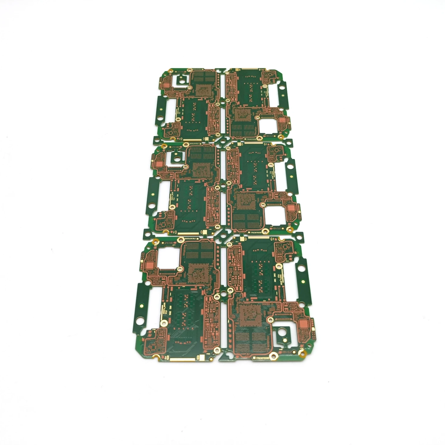
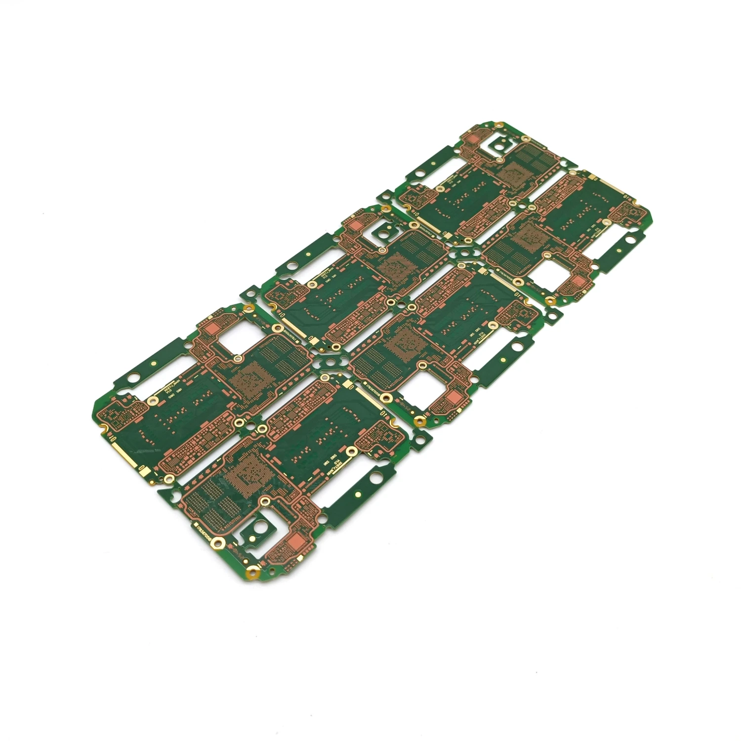
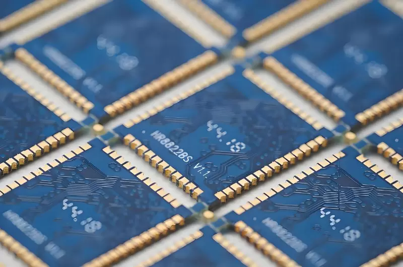
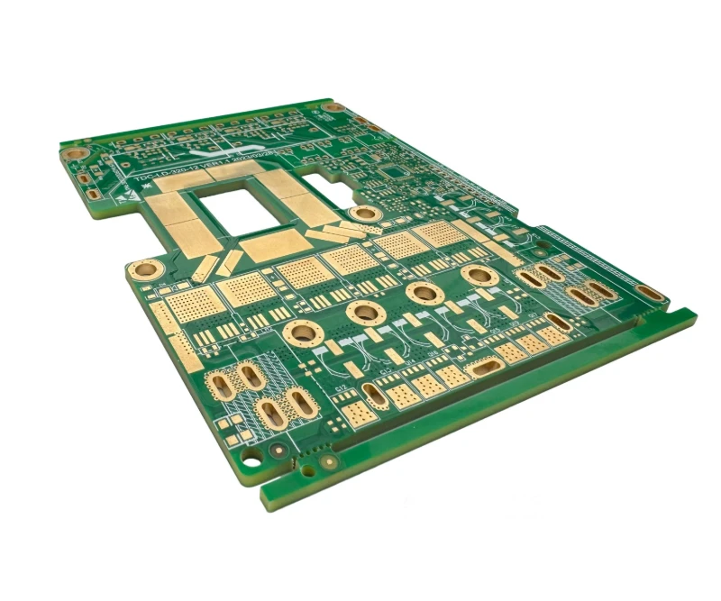
Benlida Circuit is a leader in hdi pcb solutions. Their technology gives you ultra-fine traces and microvias as tiny as 50μm. You can fit up to 10 times more parts on one board. Benlida’s hdi pcb uses special materials. These help signals move faster and make the board more reliable. You get a board that is smaller, stronger, and works better.
Why the Differences Matter
It is important to know why these differences matter for your product. Picking the right type can make your device faster, more reliable, and easier to build. Here is what you get with pcb hdi technology:
You save space and weight. This is great for wearables, smartphones, and medical devices.
You can fit more parts, so your device does more without getting bigger.
You get better signal quality and less interference. This is because of advanced materials and design.
You can use high pin count and small pitch devices. These are common in new electronics.
You need fewer layers. This can lower costs and make building easier.
If you want your product to be special, you need the right technology. Benlida Circuit’s hdi pcb gives you an advantage. Their boards meet strict rules for reliability and performance. You can trust them for things like consumer tech, cars, and airplanes.
Tip: Always pick the pcb that fits your product’s needs. If you need small size, high speed, and reliability, pcb hdi technology is the best choice.
Traditional PCB Manufacturing
Process Basics
You want your pcb to work well. You also want it to last a long time. Making a traditional circuit board uses many steps. Each step helps shape the board. Each step adds features you need. When you pick a traditional circuit board, you use proven ways. Here is a table that shows the main steps:
Step Number
Step Description
1
Inner Layer Imaging
2
Inner Layer Etching
3
Resist Stripping
4
Inner Layer AOI
5
Inner Layer Oxide
6
Layup
7
Lamination
8
X-Ray Alignment
9
Drilling
10
PCB Plating
11
Outer Layer Imaging
12
Outer Layer Etching
13
Outer Layer AOI
14
Solder Mask Application
15
Silkscreen Application and Surface Finish
16
Finishing the PCB
The process uses imaging, etching, drilling, and plating. Each step helps make strong connections. Each step helps signals stay clear. Watching the process closely helps you work better. You waste less and get a better board. If you follow these steps, you get a circuit board that works for many basic jobs.
Materials and Structure
You want your pcb to have good materials. The structure depends on what you pick. Here is a table with common materials and their properties:
Material Type
Structural Properties
PTFE
High chemical inertness, withstands temperatures up to ~250 °C, needs fillers for strength and stability.
Ceramic Substrates
Superior thermal performance, high thermal conductivity, rigid structure.
High-Speed Epoxy
Modified resins, lower Dk and Df, supports high-speed designs, higher Tg than FR-4.
Metal-Core PCBs
Thin dielectric layer on thick metal base, lowers thermal resistance, improves thermal management.
CEM Materials
Low-cost laminates, higher Dk, more moisture absorption, less performance than FR-4.
Liquid Crystal Polymer
Low Dk, very low loss, stable over wide frequency range, ideal for high-frequency uses.
You pick materials based on your project. PTFE works for high heat. Ceramic substrates make strong boards. Metal-core pcbs help with heat problems. CEM materials cost less but do not work as well. Liquid crystal polymer gives stable signals for high-frequency jobs. The way you layer and connect these materials shapes your board.
Common Uses
You want your pcb to match your project. A traditional circuit board works in many places. You see it in:
Consumer electronics like phones, computers, and home gadgets.
Car systems such as screens, navigation, and audio devices.
Factory equipment, measuring tools, and power systems.
Medical devices like monitors, scanners, and controls.
Aerospace equipment for checking and testing.
You pick a traditional circuit board for everyday products. The process gives you a board that works in many areas. You get a solution that people trust.
Tip: If you want a simple and cheap pcb for common devices, the traditional circuit board process is the best choice.
Limitations
You want your product to be different. You need a pcb that fits your needs. Traditional pcb manufacturing is reliable, but it has limits. These limits can slow your design. They can stop your ideas from growing. If you want to make something new, you should know these limits.
Here are the main problems with standard pcb technology:
Limitation Type
Description
Manufacturing Constraints
Traditional PCB manufacturing faces resolution limits that hinder the production of high-density interconnect (HDI) PCBs.
Via Limitations
Standard PCBs impose restrictions on via sizes and locations, affecting signal routing and power distribution.
Routing Complexity
Increased components and layers complicate routing, raising costs and design complexity.
Component Size
Standard technology struggles to accommodate very small components required in modern electronics.
Board Dimensions
Smaller PCBs face challenges in fitting components without compromising functionality.
Board Thickness
Non-standard thickness can affect flexibility, weight, and manufacturing costs.
Limited Material Choices
Common materials like FR4 may not meet high-performance requirements for certain applications.
Thermal Management
Thin PCBs may poorly regulate temperature, risking overheating with high-power components.
Signal Interference
Tighter component packing increases the risk of signal interference, affecting high-frequency designs.
Impedance Control
Traditional layouts struggle with impedance control, leading to signal reflection and distortion.
You notice these problems when you try to make your pcb smaller. You also see them when you add more parts. Standard pcb methods use bigger vias and thicker boards. This makes it hard to fit tiny chips. It is tough to use high pin count devices. If you want to design a pcb for a smartphone, you may have trouble with space. Signal quality can also be a problem.
Material choices are limited. Most traditional pcb boards use FR4. FR4 works for many jobs, but it does not support high-speed signals. It does not handle extreme temperatures well. If your device needs to run fast or stay cool, you may need better materials. You want your pcb to last longer. You want it to work in tough places. Standard options may not be enough.
Routing gets harder with more layers and parts. You spend more time and money to make sure signals go to the right place. You risk signal interference. Impedance control can be poor. Your pcb may not work well at high speeds. You want your device to be reliable, but these limits can cause problems.
Thermal management is another issue. Thin pcb boards may not handle heat from strong chips. Your device can get too hot and stop working. You want to avoid repairs and unhappy customers.
Note: If you want to make your design better, you should look past traditional pcb manufacturing. Advanced solutions like HDI technology help you break these limits and build better products.
Advanced HDI PCB Technology
What is Advanced HDI PCB
You want your products to be special. Advanced hdi pcb helps you do this. This technology uses high-density interconnect. It puts more power in less space. You get thinner boards and lighter devices. You also get more features. Advanced hdi pcb lets you fit over 20 parts in one square centimeter. The board can be only 0.4mm thick. You can make your device weigh 30% less. This makes your devices smaller and easier to carry.
Here’s a table that shows how advanced hdi pcb is different from standard pcb:
Feature
Advanced HDI PCB
Standard PCB
Size and Weight
Thickness reduced to 0.4mm, weight reduction >30%.
Conventional thickness ≥1.0mm, heavier.
Component Density
Supports 20+ components/cm².
Density typically ≤5 components/cm².
Drilling Technology
Laser microvia diameter 50-100μm.
Mechanical through-hole diameter ≥0.2mm.
Manufacturing Cost
Unit price 30-50% higher, but system-level savings.
4-layer bulk price $0.5-2/sheet.
Manufacturing Complexity
Requires 5+ lamination cycles.
Standard PCB: 1-2 cycles.
High-Frequency and Thermal Management
Dk ≤3.5, supports 28GHz.
Dk ≥4.5, significant losses above 10GHz.
Reliability Data
Passes 3,000 thermal cycles.
Passes 1,500 thermal cycles.
You can see the difference. Advanced hdi pcb technology lets you make smaller and faster products. Your devices are also more reliable. You can use this technology for high-speed and high-performance needs.
Manufacturing Techniques
Microvias and Laser Drilling
You want strong connections in your pcb. Microvias help you do this. These tiny holes are made by laser drilling. They connect layers and do not use much space. Laser drilling makes microvias as small as 50μm. This gives you more room for parts. It also helps with routing. You get very accurate hole placement. This keeps your signals clear. Laser drilling lets you make complex patterns. You can fit more features in your device.
Improvement Aspect
Measurement/Value
Throughput with advanced laser
4,500 holes per second
Position accuracy
Less than +/-10 μm
Diameter of through-holes
<100 μm
Microvias help your device work better. High-speed signals stay clear and strong. Your device works well even when it is small.
Build-Up Layers
You want your pcb to have more features. Build-up layers help with this. In advanced hdi pcb, you add layers one by one. This is called sequential lamination. It helps lower costs and makes your board more reliable. You can add more connections without making the board thicker. This method also keeps your signals clear. Your device stays dependable as you add more parts.
Materials for HDI
You want your advanced hdi pcb to work its best. Good materials help a lot. Using Megtron 7(G) instead of FR4 lowers dielectric loss. Rogers laminates lower the dielectric constant. This helps your device work faster. These changes keep your signals clear and strong.
Material Type
Contribution to Performance
Advanced PCB Material
Enhances thermal management and reliability in HDI PCBs
Megtron 7(G)
Reduces dielectric loss, improving signal integrity at high frequencies
Rogers Laminates
Lowers dielectric constant, shifting focus to manageable copper losses for high-frequency applications
You get more than just speed. Advanced materials help with heat and make your board last longer. Your pcb works well in tough places. You can trust your advanced hdi pcb to do a great job.
Tip: Pick advanced hdi pcb technology for your next project. You get smaller size, faster speed, and better reliability.
Application Areas
You want your products to be the best. Advanced hdi pcb helps you do this. This technology works in many industries. It is used where reliability and performance are important. You find advanced hdi pcb in medical devices and industrial control systems. It is also in military equipment, aircraft, power supplies, and auxiliary systems. Each field needs boards that are strong and work well in tough places.
Here is a table that shows how advanced hdi pcb is used:
Application Area
Description
Key Differences from Traditional PCBs
Medical Devices
Used in devices like pacemakers and defibrillators.
Needs high reliability and durability.
Industrial Control Systems
Sensors, actuators, and controllers for machines.
Gives better reliability and lower maintenance costs.
Military Applications
Used in aviation equipment, tanks, and missiles.
Resists shock and vibration better.
Aircraft Applications
Used in aircraft systems for durability and EMI resistance.
Handles strong vibrations without losing performance.
Power Supplies
Used in motors and transformers.
Manages heat from components well.
Auxiliary Systems
Used in pumps and compressors.
Resists vibrations more than regular PCBs.
You want your pcb to work where it cannot fail. Advanced hdi pcb gives you that trust. These boards last longer and work better. You can use them in important devices and harsh places.
Unique Benefits
You want your products to work really well. Advanced hdi pcb gives you special benefits. Traditional boards cannot do these things. You get very thin traces, microvias, and lots of parts on one board. These features help your pcb handle fast signals and hard designs. You get better signal quality, stronger power, and less interference.
Here is a table that shows the special benefits of advanced hdi pcb:
Benefit
Explanation
Signal Integrity
Controlled impedance keeps signals clear and strong.
Signal Reflection
Less reflection means signals stay good.
EMI Reduction
Less electromagnetic interference means better performance.
Power Delivery
Power goes to parts without loss or problems.
Reliability
Signals and power stay strong, so the board is reliable.
You want your pcb to keep signals strong. Advanced hdi pcb does this for you. You get less signal loss and better connections. Your devices run faster and use less power. You also have fewer problems with heat and shaking.
Benlida Circuit uses advanced hdi pcb to make boards with very thin lines and spaces. They use laser-drilled microvias as small as 50μm. You can connect any layer. You can fit over 5,000 parts in a tiny space. Signal loss is less than 0.2dB at 40GHz. You get ±3% impedance control and buried layers to lower EMI. These features make your products ready for new technology.
Tip: Pick advanced hdi pcb for your next project. You get the best reliability, speed, and performance. Your products will be ahead of others.
Comparing Performance and Cost
Design Complexity
You want your product to be special. The design complexity of your pcb matters a lot. Traditional boards use simple layouts and bigger traces. You run into problems when you add more features. Making your device smaller is hard. You spend extra time routing signals and placing parts. Mistakes happen more often. Sometimes, you need more layers to fix issues.
Advanced hdi pcb helps you design better boards. You use microvias and very thin traces. You connect layers in new ways. You fit more functions into less space. High pin count chips and tiny parts are easy to use. Your boards are thinner and lighter. You need fewer layers, so your design is simpler.
Benlida Circuit’s advanced hdi pcb lets you design with ease. Their technology supports complex patterns and fast signals. You avoid problems from old layouts. Your board matches your ideas and works well.
Tip: If you want to build something new and strong, pick advanced hdi pcb. You make your design easier and open up more options.
Component Density
You want your pcb to do more in a small space. Component density means how many parts fit on your board. Traditional boards have less density. You use bigger footprints and regular vias. It is hard to fit everything, especially in small devices.
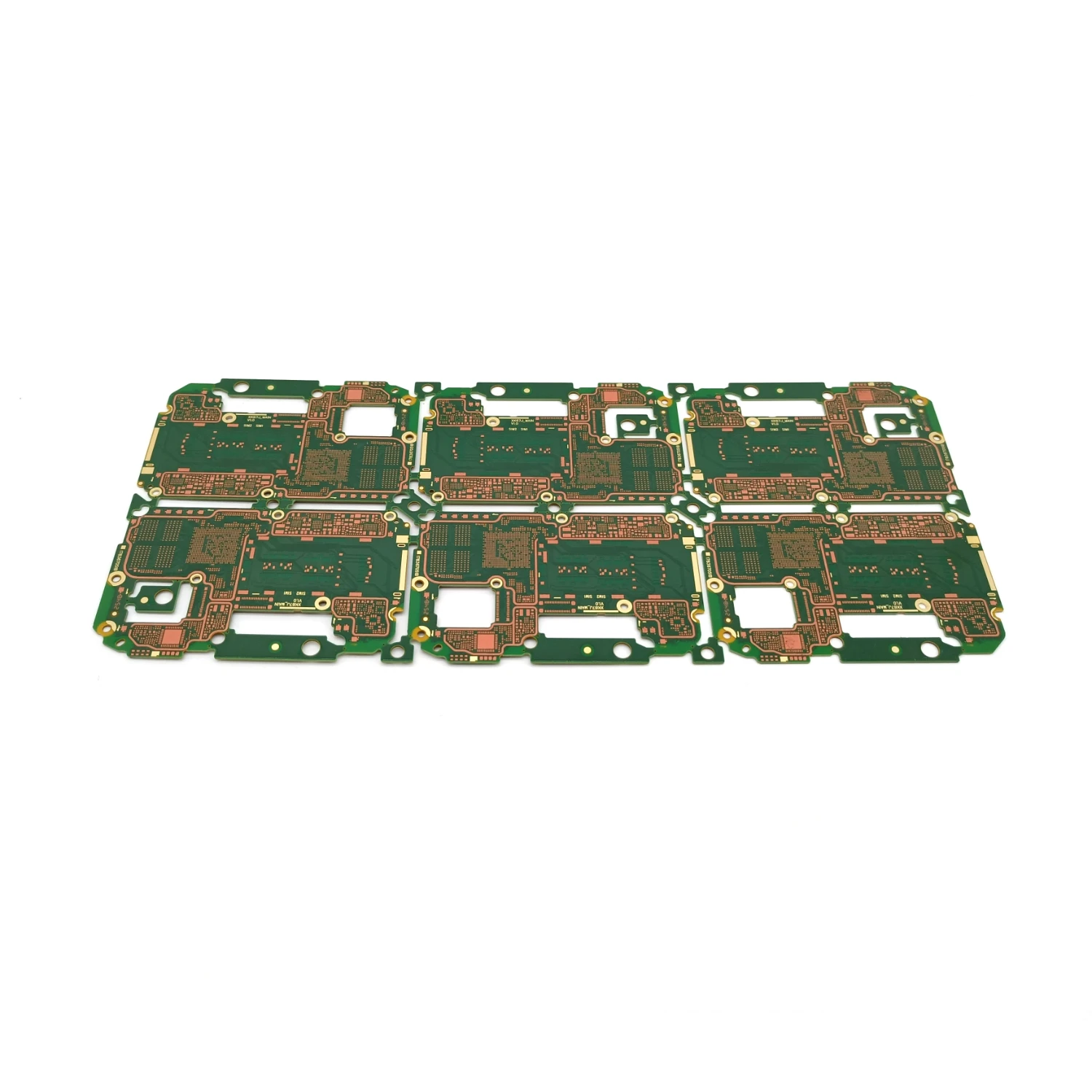
Advanced hdi pcb gives you much higher density. You use blind, buried, and microvias. Parts are closer together. Your board gets smaller but has more features. You can fit up to 20 parts in one square centimeter. You use up to 20 layers or more. Traditional boards only go up to 16 layers.
Here’s a table that shows the difference in component density:
Feature
Traditional PCBs
HDI PCBs
Number of Layers
Up to 16 layers
20 layers or more
Via Design
Standard drilled vias
Blind, buried, micro vias
Component Density
Lower density
Higher density
Size
Larger footprint
Compact form factor
You see the benefit. Advanced hdi pcb lets you make smaller and smarter products. You fit more technology into every inch. You lead the way in making tiny and advanced devices.
Manufacturing Process
You want your pcb to be reliable and not cost too much. The way you make your board changes how fast you get it and what you pay. Traditional boards use mechanical drilling and regular lamination. Most jobs finish in one or two cycles. These methods are old and work well. You pay less, but you cannot do as much with your design.
Advanced hdi pcb uses a new process. You use laser drilling for microvias. You add layers one by one, sometimes five or more cycles. Special machines handle tiny spaces. Via-in-pad technology makes things harder but improves performance. You pay more at first, but you save money by using fewer layers and making your system work better.
Advanced hdi pcb costs 30-50% more than standard boards.
Microvia copper filling has defect rates below 0.1%, so failures are rare.
Advanced hdi pcb passes thermal tests up to 3,000 cycles. Traditional boards pass only 1,500.
You spend more to make the board, but you get better results.
Benlida Circuit’s advanced hdi pcb uses high-quality processes and new technology. Their boards have very thin traces and microvias as small as 50μm. You get a defect-free rate of 99.95% for microvias. You can trust your board in tough places.
Note: If you want the best results, choose advanced hdi pcb. You get a process that gives you better performance, more reliability, and good value for your money.
Cost Factors
You want to keep your project costs low. The price of your pcb depends on many things. HDI technology costs more at first, but it works better. More layers in your pcb make it cost more. Each layer means extra work and higher prices. Complicated via structures also make the price go up. If you pick special materials or need your pcb quickly, you pay more.
Here is a table that shows what affects the cost:
Cost Factor
Impact on Cost
Number of Layers
More layers mean more steps and higher cost.
Via Structure
Complicated vias make building harder and cost more.
Material Type and Turnaround Time
Special materials and fast orders cost extra money.
Cost Comparison
HDI PCBs can cost 2 to 5 times more than regular PCBs, but the price is worth it.
HDI pcbs cost more, but you get a smaller and faster product. You save money later because you use fewer layers and get more features. Benlida Circuit helps you spend less by using smart methods and good materials. You get a strong pcb that does what you need.
Tip: For the best value, pick hdi pcb for your next project. You pay more now, but you save money on fixes and upgrades later.
Performance Metrics
You want your pcb to work really well. You need to check important performance numbers. These numbers show how your board handles signals, speed, and how long it lasts. HDI pcbs use microvias and very thin lines. This helps your device run faster and lose less signal. You get better results for fast and high-frequency jobs.
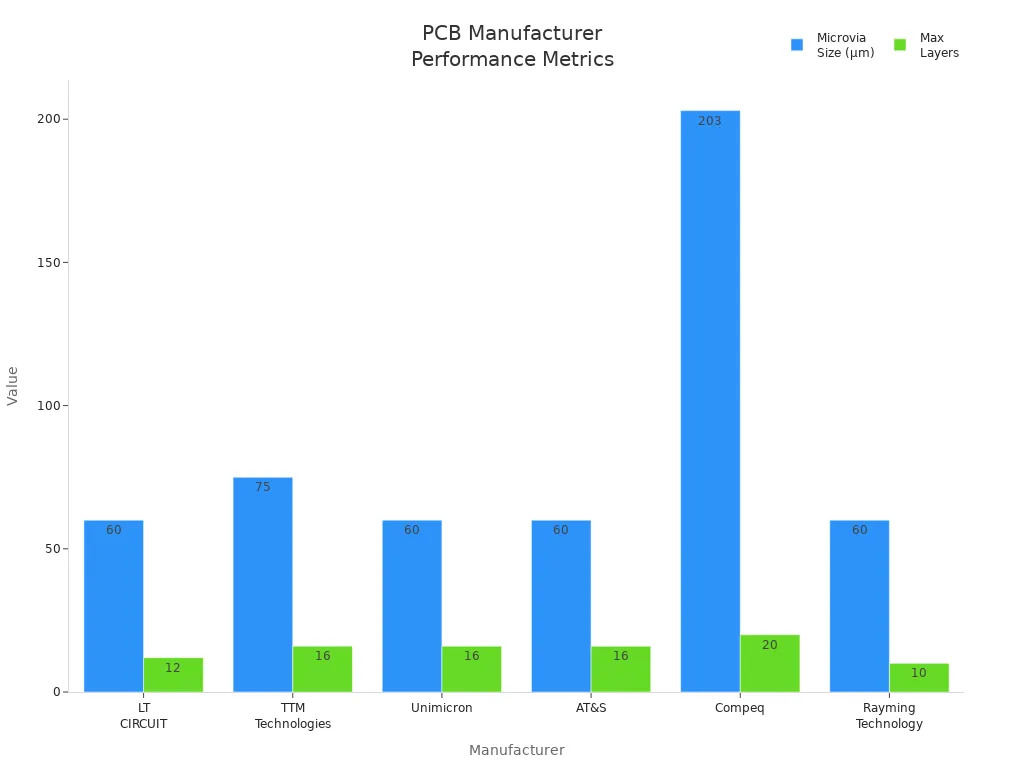
Here is a table that compares top makers and their pcb performance:
Manufacturer
Microvia Size
Max Layers
Trace/Space
Industry Focus
Lead Time (Prototypes)
LT CIRCUIT
60μm
12
3/3 mils
Aerospace, medical, telecom
5–7 days
TTM Technologies
75μm
16+
3/3 mils
Aerospace, defense
7–10 days
Unimicron
60μm
16
3/3 mils
Consumer electronics, automotive
5–8 days
AT&S
60μm
16
<4 mils
Automotive ADAS, EV
8–12 days
Compeq
203μm
20
4 mils
Telecom, data centers
10–15 days
Rayming Technology
60μm
10
2/2 mils
IoT, prototypes
4–6 days
HDI pcb technology uses smaller microvias and more layers. This lets you build better and smarter products. You get faster delivery and stronger boards. Benlida Circuit’s hdi pcb uses microvias as tiny as 50μm and supports up to 20 layers. You get very thin lines and lots of parts on one board. Your device runs faster and does more things.
Note: For top performance, choose hdi pcb. You get better signals, speed, and reliability.
Reliability
You want your pcb to last a long time. Reliability is important for every project. HDI pcbs use special materials and smart building steps. This makes your board stronger and less likely to break. Microvias and buried vias help stop cracks and breaks. You get better results in tough places.
Here is a table that shows how reliability is different:
Aspect
HDI PCBs
Traditional PCBs
Structural Differences
Use micro blind/buried via technology
Use regular multilayer structures
Material Differences
Use strong dielectrics with low CTE
Use regular FR-4 materials
Process Differences
Use many lamination steps and careful work
Use simple building steps
Failure Mode Differences
Problems happen at microvia connections
Problems happen from through-hole breaks
HDI pcbs from Benlida Circuit pass over 1,000 heat cycles. You get a defect-free rate of 99.95% for microvias. Your board can handle heat, shaking, and bumps. You avoid problems like broken solder and lost signals. Your device stays strong in any place.
Tip: If you want your product to last, pick hdi pcb. You worry less and fix things less often.
Application Scenarios for PCB HDI Technology
When to Use Traditional PCBs
You need to pick the right pcb for your project. Traditional pcb technology is good for simple and cheap products. You get steady performance without paying for extra features. If your design does not need lots of parts or fast signals, you save money and time with this choice.
Here is a table that shows where traditional pcb technology works best:
Application Type
Description
Consumer Electronics
Good for TVs, washing machines, and basic gadgets
Industrial Automation
Used in many factory systems
Automotive Systems
Common in car screens and power controls
Cost Constraints
Great for simple, low-cost projects
Tip: Use traditional pcb technology when you want a trusted and low-cost solution for everyday products.
When to Use Advanced HDI PCB
You want your product to be special. Advanced HDI pcb technology gives you more power in less space. Pick this when your design needs lots of parts, small size, or fast signals. You also get better reliability and clearer signals. This technology lets you use special materials and new via types.
Use advanced HDI pcb when:
You need to fit many parts in a small space.
Your device must be thin and light.
Your design needs fast signals.
You want better reliability and strong signals.
You need special materials and tricky via designs.
Benlida Circuit’s HDI pcb helps you make new and smart products. You can build smartphones, wearables, and AI hardware that lead the market.
Industry Examples
Consumer Tech
You want your devices to be smaller and smarter. HDI pcb technology makes this happen. You see it in laptops, cameras, and new smartphones. Benlida Circuit’s HDI pcb lets you add more features to wearables and smart gadgets. Your products get lighter and stronger.
Medical Devices
You need medical devices to be safe and work well. HDI pcb technology is used in things like pacemakers and portable X-ray machines. You get small designs that work in important moments. Benlida Circuit’s HDI pcb meets tough rules for medical use, so you feel safe.
Automotive
You want cool features in cars. HDI pcb technology powers WiFi, maps, and safety systems in cars. Your car products get smarter and more connected. Benlida Circuit’s HDI pcb works in hard conditions, so your systems stay strong on the road.
Aerospace
You need strong and light boards for planes. HDI pcb technology is used in cockpit controls and other systems. Your aerospace products get high reliability and less weight. Benlida Circuit’s HDI pcb gives you performance you can trust, even in tough places.
Note: Pick the right pcb for your industry. Advanced HDI pcb from Benlida Circuit helps you lead in technology, safety, and new ideas.
Choosing the Right PCB Solution
Design Needs
You want your product to be different. Your design needs help you pick the best pcb technology. If you want a device that is small and strong, look at advanced choices. Small size is important for smartphones and wearables. Good signal quality matters for telecommunications and IoT devices. More features help medical devices and car electronics. Small shapes are needed for aerospace and defense systems. Fast computers need advanced solutions for AI hardware.
Here is a table that shows how design needs match different application areas:
Design Need
Application Area
Miniaturization
Smartphones, Wearable Devices
High Signal Integrity
Telecommunications, IoT Devices
Increased Functionality
Medical Devices, Automotive Electronics
Compact Form Factors
Aerospace and Defense Systems
High Performance Computing
HPC and AI Hardware
You should match your design needs to the right pcb solution. If your project needs more features in less space, HDI pcb technology is a good choice.
Budget and Timeline
You want your project to finish on time and not cost too much. Planning your budget and timeline early helps you avoid problems. How many boards you need changes your choice of manufacturer. This affects cost and how fast you get your boards. You need to know how price and quality work together. Managing your money and time is important in pcb design. Checking your budget and schedule often helps you balance quality and cost.
Make sure your budget and quality needs are clear from the start.
How many boards you need changes your choice of manufacturer, cost, and timeline.
Knowing how price and quality connect helps you make smart choices.
Use your resources wisely to keep costs low.
Set a clear schedule with goals to track progress and finish on time.
You save money and time when you plan well. You get a pcb that fits your needs without problems.
Supplier Capabilities
You want a supplier who can give you what you need. The right supplier helps your pcb project succeed. Careful part placement keeps mistakes low. Good equipment care means fewer problems and faster work. Preventing defects helps you avoid expensive errors. Saving money helps your business and reputation.
Top suppliers like Benlida Circuit have strong manufacturing skills. They make complex boards and work with tiny parts. Their quality checks keep defect rates below 1%. They have certifications like ISO 9001 and RoHS. You get many pcb assembly services, like parts buying, testing, and making samples. Fast work and the ability to handle big orders help you meet tight deadlines. Helpful support and clear updates keep you informed and confident.
Careful part placement
Good equipment care
Defect prevention
Saving money
Making complex boards
Strong quality checks
Important certifications
Many assembly services
Fast work and big order handling
Helpful support
You should pick a supplier who meets these standards. Your pcb project will go well and give you the results you want.
Future-Proofing
You want your product to last and stay ahead of new trends. When you choose a pcb for your design, you must think about future-proofing. This means you prepare your product for changes and upgrades. You make smart choices now so your device works well later.
Start by making sure your team works together. Everyone should know the plan for your pcb. Over-communicate with all departments. This helps you catch problems early and keeps your project moving. You need engineers, designers, and managers to share ideas. Collaboration leads to better results.
Think about the size of your product. The market wants smaller devices. Design your pcb to fit tight spaces. Use multiple layers and build vertically if you need more room. This lets you add new features without making your device bigger.
Look at the parts you use. Some components, like microcontrollers and sensors, may need upgrades. Choose modular connectors so you can swap parts easily. Add unused pads or mounting holes for future additions. You give yourself options for new technology.
Consider how your pcb will be used. If your device faces tough conditions, pick strong materials and smart mechanical structures. Decide if your application is static or exposed to outside forces. This affects your design choices and helps your product last longer.
Here are steps you can follow to future-proof your pcb:
Identify which components may need upgrades in the future.
Use modular connectors for easy changes.
Include extra pads or mounting holes for new parts.
Work with all departments to optimize layout and manage space.
Prepare for space limits by using more layers and vertical building.
Tip: Always plan for growth. Your pcb should support new features and upgrades. This keeps your product valuable and ready for the future.
You want your device to stand out. By future-proofing your pcb, you make sure it stays useful and strong. You save money and time when you update your product. You also keep your customers happy with new options and better performance.
You have two ways to make a pcb. One way is traditional, and the other is advanced HDI. The main differences are wiring density, microvias, and how well the board works. Look at this table to see how they compare:
Aspect
Traditional PCB Manufacturing
Advanced HDI PCB Manufacturing
Wiring Density
Lower
Higher
Via Types
Standard
Microvias, blind, buried
Performance
Basic
Enhanced
HDI technology lets you make smaller boards. It also gives better electrical performance. Think about what your project needs for size and speed. HDI pcb is good for small and fast designs. Make sure your files are clear and you follow the rules. If you need help, ask Benlida Circuit for custom pcb solutions.
FAQ
What is the main advantage of HDI pcb technology?
HDI pcb lets you fit more parts in less space. It helps you make devices that are smaller, lighter, and faster. Your products work better and stand out in high-tech markets.
Can I use HDI pcb for any electronic device?
HDI pcb works for most new devices. It is best for smartphones, wearables, medical sensors, and AI hardware. If you want strong performance and reliability, HDI pcb is a good choice.
How does HDI pcb improve signal quality?
HDI pcb uses microvias and special materials. These keep signals clear and strong. You get less interference and faster speeds. Your device works better in tough places.
Is HDI pcb more expensive than traditional pcb?
HDI pcb costs more at first. You save money later because you need fewer layers and get better results. Your products last longer and break less often.
Why should I choose Benlida Circuit for my pcb needs?
Benlida Circuit gives you advanced HDI pcb solutions. You get very thin traces, lots of parts, and strong boards. Their technology helps your products lead in new ideas and quality.
How do I know which pcb type fits my project?
Look at what your design needs. If you want simple and cheap, pick traditional pcb. If you need small size, speed, and reliability, choose HDI pcb. Benlida Circuit can help you pick.
What industries benefit most from HDI pcb?
Consumer tech, medical devices, cars, and airplanes use HDI pcb. These fields get better performance, smaller products, and stronger boards.
Tip: Always ask your supplier which pcb is best for your project. You get better results when you pick the right technology.
This website uses cookies to provide you with a safer and more personal experience. By accepting, you agree to the Cookie Policy and the use of cookies for advertising and analytics purposes.
 en
en

 WhatsApp