Case Study: Wireless Keyboard PCB Assembly — Engineering Precision for Seamless Typing Experiences
In the era of remote work and digital productivity, wireless keyboards have become essential tools, demanding reliable connectivity, long battery life, and responsive performance. A leading computer peripherals brand partnered with us to address key challenges in assembling PCBs for their premium wireless mechanical keyboard, focusing on low-latency connectivity, power efficiency, and durable key actuation.
Project Background & Client Requirements
The client’s keyboard is a full-size wireless mechanical model featuring Bluetooth 5.2 and 2.4GHz RF connectivity, targeting professional users and enthusiasts. Its main PCB needed to:
· Support ultra-low latency (<10ms) between key presses and device response for gaming and fast typing.
· Integrate 104 mechanical key switches with debounce circuitry to ensure accurate input recognition.
· Operate on 2 AA batteries for 12+ months (based on 4 hours of daily use) to minimize recharging.
· Withstand 50+ million key presses without electrical failure, meeting premium durability standards.
· Scale from prototype (150 units) to mass production (5,000 units/month) with consistent quality (PPM ≤15).
Key Challenges in Wireless Keyboard PCB Assembly
The project presented unique hurdles tied to the keyboard’s wireless functionality and mechanical demands:
1. RF Signal Stability: Bluetooth and 2.4GHz RF modules must maintain consistent connectivity despite interference from nearby electronics (e.g., Wi-Fi routers, smartphones).
2. Low-Power Optimization: Even minor current leakage in PCB traces or components could drastically reduce battery life, falling short of the 12-month target.
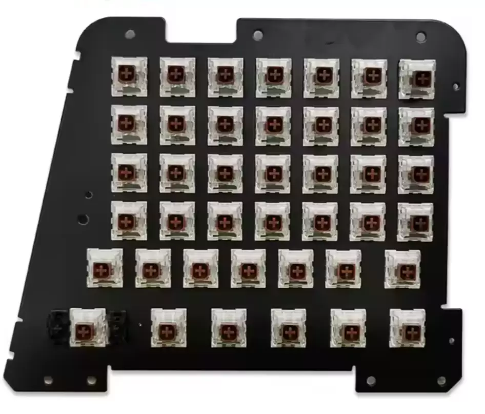
3. Mechanical Durability: Solder joints for key switch pins and connectors must withstand millions of actuations and occasional drops without failure.
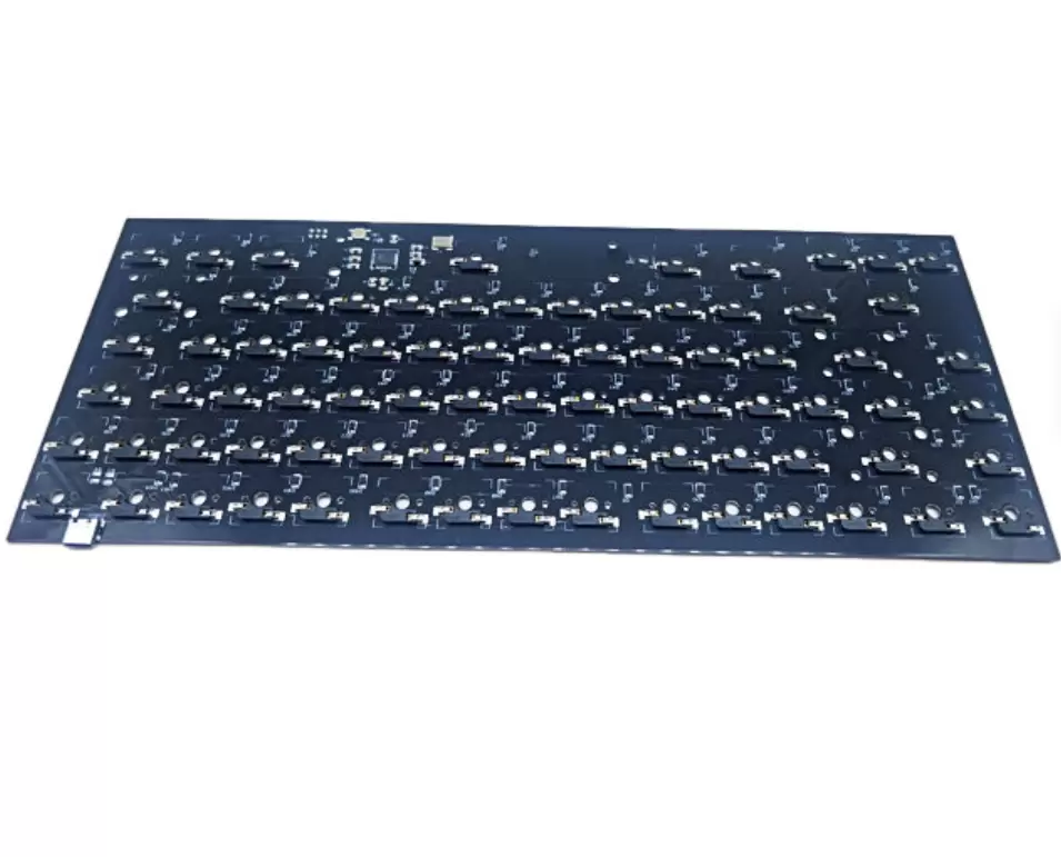
4. Compact Layout Complexity: Fitting 104 key switch contacts, a microcontroller, wireless modules, and LED backlighting into a slim (≤3mm thick) PCB requires high-density routing.
Our Tailored Assembly Solutions
To overcome these challenges, we developed a “efficiency + durability” strategy combining RF optimization, power management, and precision assembly:
1. PCB Design & Power Optimization
· Layout Engineering:
· Segregated RF circuits (Bluetooth module, 2.4GHz antenna) from digital key matrix circuits with grounded copper planes to minimize interference.
· Designed a star topology for the key matrix to reduce trace length, ensuring <5ms signal propagation from any key to the MCU.
· Integrated a low-power MCU (32-bit ARM Cortex-M0+) with deep-sleep mode (<5μA current) to maximize battery efficiency during idle periods.
· Material Selection:
· Used 2-layer high-Tg (150°C) FR-4 substrate with 1oz copper for optimal current handling and mechanical rigidity in a slim form factor.
· Applied ENIG (Electroless Nickel Immersion Gold) surface finish on key switch pads to ensure consistent electrical contact over millions of presses.
· Power Distribution:
· Routed power traces with 0.2mm width to minimize resistance while keeping the PCB slim, with separate power paths for high-current components (e.g., LED backlights) to avoid voltage drops.
2. Precision Assembly for Reliable Performance
· SMT for Control and Wireless Components:
· Employed Yamaha YSM10 pick-and-place machines with vision alignment (±5μm accuracy) to place the Bluetooth module, MCU, and 0402 passives, ensuring precise positioning for RF signal integrity.
· Used a laser-cut stencil (0.12mm thickness) to apply solder paste evenly on fine-pitch components (e.g., 0.5mm QFN MCU), with 3D SPI verifying paste volume (±10%) to prevent bridging.
· Through-Hole Assembly for Key Switches:
· Inserted and soldered mechanical key switch pins (2.54mm pitch) using wave soldering with a low-temperature profile (230°C peak) to avoid damaging the plastic switch housings.
· Inspected each switch solder joint via AOI to ensure full wetting and mechanical strength, critical for withstanding millions of actuations.
· Connector and Antenna Integration:
· Soldered the 2.4GHz PCB antenna with precise orientation (90° to the board edge) to maximize signal range, then secured it with UV-cured adhesive for vibration resistance.
· Added a gold-plated battery connector with spring contacts to ensure reliable power delivery even with minor battery movement.
3. Rigorous Testing & Reliability Validation
· Wireless Performance Testing:
· Measured latency via custom software (average <8ms for both Bluetooth and 2.4GHz) and verified connection stability in crowded RF environments (10+ nearby wireless devices).
· Tested wireless range (>10m for Bluetooth, >15m for 2.4GHz) to ensure flexibility in workspace setup.
· Power Efficiency Testing:
· Monitored current draw in active (3mA) and sleep (4μA) modes using a precision ammeter, confirming the 12-month battery life target with 20% margin.
· Validated low-power modes by simulating idle periods (up to 8 hours) and verifying instant wake-up (<100ms) when a key is pressed.
· Durability and Mechanical Testing:
· Conducted key press testing (100,000 cycles per switch) using automated actuators, with electrical continuity checks after every 10,000 cycles to ensure no contact degradation.
· Performed drop tests (1m onto hardwood) and vibration testing (10-500Hz) to simulate real-world handling, followed by functional checks for switch and wireless performance.
Project Outcomes & Client Impact
· Typing Performance: The PCBs enabled ultra-low latency (<8ms) and 100% key recognition accuracy, even during rapid typing (100+ words per minute).
· Battery Life: Field testing confirmed 14+ months of use on 2 AA batteries, exceeding the client’s 12-month target and boosting customer satisfaction.
· Production Scalability: Scaled from 150 prototypes to 5,000 units/month with 99.5% yield, supported by automated testing that reduced inspection time by 60%.
· Durability: All tested units passed 50+ million key press simulations with no electrical failures, meeting the client’s premium quality standards.
Why Choose Us for Wireless Keyboard PCB Assembly?
Wireless keyboard PCBs demand expertise in RF optimization, low-power design, and mechanical durability—areas where our 14-year focus on consumer electronics assembly excels. We understand that every key press matters, and our processes are designed to deliver PCBs that ensure responsive, reliable performance for years of use.
 en
en


 WhatsApp