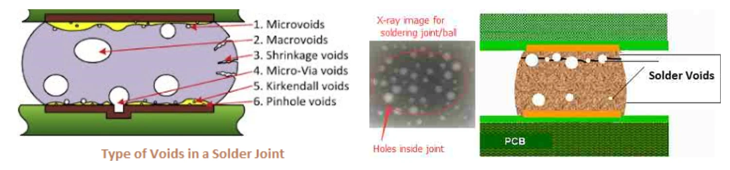
Definition: Voids in solder joint, refers to holes, bubbles, gaps, open pockets, empty spaces, inside of the solder joint. Solder void is typically generated by entrapped gasses/vapour or paste flux residues, that were not able to emit/release from solder joint during the reflow process.
What factors might cause solder voiding:
● Solder Paste
● Stencil
● PCB Surface Finish
● Moisture of PCB and Components
● Process Environment/Reflow Temperature
Negative impact and potential risks of solder voids
● Decrease the reliability of solder joint
● Reduce the thermal conductivity of solder joint
● Decrease the current carrying capacity
● Potential physical crack/mechanical failture of solder joint

Solutions to prevent solder voiding:
1. Solder Paste
The most basic, widely applied, quick to verify and cost-effective method is to reduce the generation of gases, or vapour at the first beginning, such as applying low-void solder paste.
- Dedicated Solder Powder Alloy: Choose an alloy solder paste with low oxidation rate and good fluidity in the molten state.
- Fluoride: The rate and volume of gas generation by the flux at elevated temperatures are crucial. High-quality low-void solder paste allows the flux to release gases smoothly and slowly, and decomposes almost completely before reflow. Solder paste with a high-boiling-point solvent is preferred.
- Solder paste Comparison: Request voiding reports from solder paste manufacturers and compare
2. Optimize Stencil Opening
- Micro-etching or Stepped Stencil: Micro-etching the stencil openings, corresponding to the pads of components, such as QFN and BGA (expanding the openings), or apply a stepped stencil (thickening) to increase the amount of solder paste, cause more solder paste provides more channels to release the gas and vapour.
- Increase Emitting/Releasing Channels: Design a grid-like grid or slotted design on the opening of the stencil, corresponding to the QFN central hot-swappable pads, to avoid entrapped gas or air bubble, and create channels for gas releasing.
3. PCB and Components
- PCB surface treatment: ENIG is better than OSP, also need to ensure there is non-porous to prevent moisture from the substrate from escaping through plating pores.
- PCB and Component Baking: Before reflow soldering, bake the moisture-sensitive PCB and components at certain temperature, such as 80°C, 4-8 hours, to evaporate mositure thoroughly.
4. Reflow Soldering Process Optimization (Process Optimization)
1) Create optimal conditions for gas emitting/releasing by controlling the heating process precisely.
2) Optimize the reflow temperature profile with a sufficient, gradual preheating/activation zone: sufficient time (usually 90-120 seconds) for the solvent and some activators to evaporate, smoothly and fully, avoiding boiling caused by quick heating. The heating rate is typically controlled at 1.0-2.0°C/s.
3) Reasonable reflow peak temperature and time: Ensure the solder is fully wetted, but avoid excessively high temperatures and excessively long reflow times, otherwise it will exacerbate solder oxidation and flux carbonization, generating new gases. The time above the liquidus line needs to be precisely set according to the component and PCB heat capacity.
4) Nitrogen-protected reflow soldering: Filling the reflow oven with nitrogen and controlling the oxygen content below 1000ppm (ideally <100ppm) significantly reduces oxidation during solder melting. Reduced oxides mean better solder flowability, more uniform surface tension, and better gas expulsion. This is currently the standard configuration for high-reliability production lines.
5. Advanced technology application (ultimate solution)
When the methods above still cannot solve the voiding issues, (such as automotive power modules requires void ratio <3%), then have to consider the ultimate solution: vacuum reflow soldering technology.
- Principle of vacuum technology: when the solder paste is in molten state, drawn a high-pressure vacuum (usually reaching 10⁻² mbar or even higher) into the oven cavity, using the pressure to extract the gas, vapour or air bubbles inside the molten solder.
- Currently, this is most effective and thorough method to reducing voids, lowering the void rate to below 1%.
- Disadvantages: Extremely expensive equipment and operating costs.
Summary and Process Recommendations:
- Material, tools and process optimization: reduces gas&vapour generation and creates extracting channels, capable to solve most common issues.
- Process Profile and Nitrogen: controls the extracting process.
- Vacuum Reflow Soldering: forces gas emitting and releasing.
Recommended Process Optimization:
1) From the materials, tools and process: low-voiding solder paste, stencils, and PCB&components baking before assembly.
2) Optimize the process: Set reflow temperature profiles, and enable nitrogen protection.
3) Professional equipment: for products which require highest-standard reliability, consider to applying vacuum reflow soldering technology.
Through this systematic approaches, the solder voiding rate could be effectively decreased.
Benlida has been manufacturing and assembling PCBs for over 14 years, with experience and professional process monitoring, it is expert to prevent solder voiding during reflow soldering, ensuring excellent and stable quality of each PCBA board.
Relating to solder voiding, our other service include:
1) Inspection of solder voiding rate: Using high-resolution 3D X-ray, standard IPC-A-610, measure the voiding ratio accurately and the locations, for BGA, QFN, and other solder joints.
2) Audit and optimization for reflow soldering process: Review and optimize the reflow soldering process and temperature profile before PCB assembly, provide optimizing solutions.
3) Assessment for solder paste performance: Compare and test key indicators of solder paste, such as voiding rate and wettability from various brands/models, from various manufacturers.
4) Analysis for failure: Analyze the reasons and assess the losses due to thermal failure, cracking, and other issues caused by voids.
 en
en


 WhatsApp