Beyond the Standard PCB: What Makes IC Substrates Different?
For decades, standard FR4-based PCBs were sufficient for most electronics. But as we transition to AI accelerators, 5G modules, and sophisticated wearable microelectronics, the physical limitations of traditional boards have become a bottleneck.
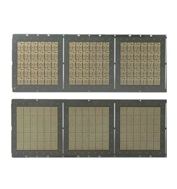
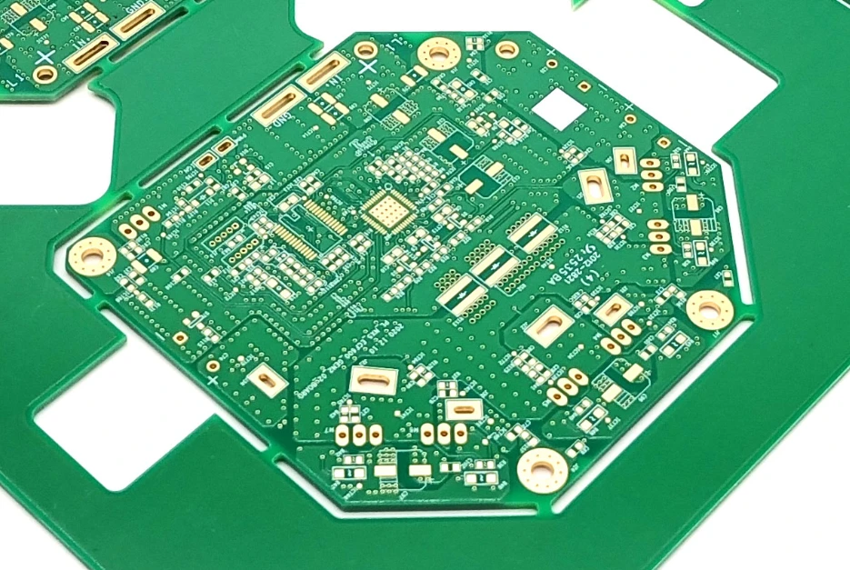
IC substrates function as a critical interface. They deliver roughly 10 times the density of a standard PCB, featuring line widths and spacing of ≤10μm and micro-bumps as small as 40μm. This level of miniaturization requires a fundamental shift in how we approach the IC substrate assembly process, moving away from basic etching toward advanced additive manufacturing and high-precision build-up techniques.
The Technical Anatomy of the IC Substrate Assembly Process
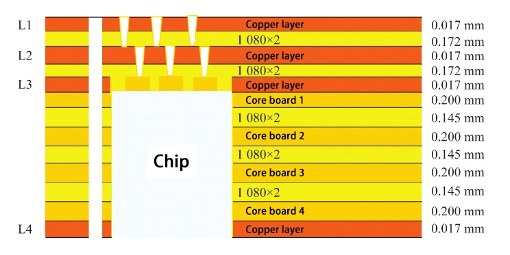
The manufacturing of an IC substrate is a multi-stage marathon of precision engineering. Unlike a standard board that might have 4 to 8 layers, advanced IC substrates often utilize 20+ build-up layers to manage the routing complexity of modern chips.
1. High-Density Build-up Structures
The core of the IC substrate assembly process involves building layers sequentially using high-density interconnect structures. These layers are not just stacked; they are engineered to route signals within an incredibly limited spatial footprint. As the layer count increases, the margin for error in alignment shrinks to nearly zero. Even a 1-micron shift in layer registration can lead to massive signal loss or internal shorts.
2. Laser-Drilled Micro-vias and Plating
To connect these 20+ layers, we rely on micro-vias. These are tiny holes, often drilled with UV or CO2 lasers, that enable vertical conductivity. During the IC substrate assembly process, these vias are filled with copper plating to ensure stable power distribution and high-speed signal transmission. Without this level of "vertical" precision, the fine-pitch interconnections required by the latest silicon dies simply wouldn't be possible.
3. Material Science: BT vs. ABF
The choice of material is a silent but vital part of the IC substrate assembly process. Most designs utilize specialized resins like BT (Bismaleimide Triazine) or ABF (Ajinomoto Build-up Film). These materials are chosen for their electrical stability and their ability to handle the fine-line circuitry that standard epoxy-glass substrates cannot support.
Application-Driven Engineering: One Size Does Not Fit All
One of the most human elements of this industry is understanding that every project has a different "soul." The IC substrate assembly process must be tailored to the specific environment where the chip will live.
1. Automotive Electronics: In a car, reliability is everything. The IC substrate assembly process for automotive applications prioritizes long-term resistance to temperature variation and mechanical vibration. These substrates aren't just built to perform; they are built to survive for 15 years in a harsh engine or chassis environment.
2. High-Performance Computing (HPC) and AI: For data centers and AI accelerators, the priority shifts to signal integrity and power distribution. These substrates must handle massive current loads without dropping voltage, requiring customized copper thicknesses (often ranging from 1/2oz to 3oz) to balance heat and efficiency.
3. Consumer Electronics: For the watch on your wrist or the phone in your pocket, the IC substrate assembly process is a battle for space. The focus here is on reducing total thickness while maintaining the integrity of dozens of functional layers.
The Invisible Challenges: Warpage and Thermal Integrity
If you speak to any engineer involved in the IC substrate assembly process, they will eventually mention "warpage". Because these boards are so thin and the layers so dense, the heat used during lamination and soldering can cause the substrate to bow or twist.
This is why precision engineering and "One-stop Turnkey" services are so important. Managing the thermal profile of the board throughout the IC substrate assembly process is the only way to ensure that the 40μm micro-bumps on the chip line up perfectly with the pads on the substrate. Before any product leaves the floor, it undergoes rigorous electrical testing and structural inspection to confirm that it remains stable under long operating hours.
Choosing the Right Partner for Your IC Substrate Project
1. Because most IC substrates are developed for specific, complex projects rather than produced as standard items, your manufacturer’s capacity for customization is key. A true partner provides:
2. Customized Parameters: Tailoring copper thickness, layer counts, and via configurations to your chip's specific routing needs.
3. Precision Finishing: Offering various surface finishes like HASL or specialized plating to match your final assembly requirements.
Advanced Testing: Utilizing high-end systems (like Debian 10-based testing rigs with 16GB RAM) to ensure every trace is perfect.
Advanced Manufacturing Horizons and the mSAP Evolution
To truly appreciate the IC substrate assembly process, one must look at the technical leap from traditional subtractive etching to the Modified Semi-Additive Process (mSAP). While conventional PCB manufacturing relies on "stripping away" copper, mSAP builds circuits from the ground up on an ultra-thin seed layer.
This is the only reliable way to achieve the dead-straight sidewalls and rectangular cross-sections required for signals hitting 112Gbps and higher. Without mSAP, the "signal noise" caused by the ragged, uneven edges of etched traces would make high-frequency AI accelerators practically useless. Operating this process requires a cleanroom environment that rivals a surgical theater; a single microscopic dust mote can snap a 10μm line, turning an entire production batch into an expensive scrap heap.
The Chemistry of Success with Electroless Plating
A successful IC substrate assembly process hinges on the delicate chemistry of electroless copper deposition. Unlike standard electroplating that uses an electrical charge, electroless plating utilizes a chemical reduction to coat surfaces with a perfectly uniform copper layer—even inside the deepest, narrowest micro-vias.
1.The Seed Layer: This acts as the bedrock for the entire circuit.
2.Adhesion Risks: If the chemical balance is off, the copper won't bond properly to the ABF or BT resin.
3.Reflow Stability: Poor adhesion leads to catastrophic delamination under the extreme heat of reflow soldering.
4.Micro Interconnects and the 40μm Pitch Challenge
In the modern IC substrate assembly process, the physical link between the silicon die and the substrate relies on micro-bumps. As we push toward a 40μm pitch, the gap between connections is now roughly half the thickness of a human hair. This leaves virtually zero margin for error regarding solder bridging.
Engineers now depend on specialized "Underfill" materials—high-tech epoxies wicked into the gap via capillary action. This underfill is vital for absorbing mechanical stress caused by Coefficient of Thermal Expansion (CTE) mismatches. It ensures that micro-bumps don't crack when a processor cycles from room temperature to 90°C in the blink of an eye.
Substrate Packaging Trends from FC-BGA to 3D Integration
The IC substrate assembly process is effectively the gateway to 2.5D and 3D packaging. In traditional Flip-Chip Ball Grid Array (FC-BGA) setups, the chip is flipped to connect directly to the substrate, cutting down inductance.
However, the industry is now pivoting toward Chiplets, where multiple small silicon dies occupy a single high-performance substrate. This "System-in-Package" (SiP) approach pushes substrate routing density to its absolute limit, often necessitating silicon interposers or ultra-thin organic substrates that challenge the laws of physics and manufacturability.
Thermal Management in High-Density Environments
With power densities in AI chips now climbing toward 700W or even 1000W, the IC substrate assembly process must double as a cooling strategy.
We achieve this by integrating "Thermal Vias"—clusters of copper-filled micro-vias that act as high-speed lanes to pull heat away from silicon hot spots and into the core layers. We are even seeing designs that embed cooling channels or heat spreaders directly into the substrate build-up. This proactive heat dissipation is the only way to prevent thermal throttling and ensure computing clusters stay at peak performance without crashing.
The Role of AOI and AI in Quality Assurance
Since the IC substrate assembly process involves millions of potential fail points on a single panel, manual inspection has become a relic of the past. We now use high-resolution Automated Optical Inspection (AOI) systems backed by AI to cross-reference manufactured boards against "golden" CAD designs in real-time.
These systems spot flaws invisible to human eyes:
1.Near-shorts: Where traces are dangerously close.
2.Plating Voids: Tiny gaps in the copper plating of a via.
3.Alignment Shifts: Sub-micron deviations in layer stacking.
This data loops back into the line to adjust laser drilling or plating settings on the fly, creating a self-correcting system that keeps yields high.
Future Proofing for 6G and Beyond
Looking toward the 2030s, the IC substrate assembly process is already bracing for 6G wireless standards. Operating at Terahertz (THz) frequencies means signal loss will be even more punishing than it is with 5G. This shift will require entirely new, ultra-low-loss dielectric materials and line-width control that likely dips below 5μm. We expect the substrate to evolve from a passive carrier into an active component, likely with antennas and RF filters integrated directly into the build-up layers.
Environmental Sustainability in Substrate Manufacturing
Finally, the IC substrate assembly process is adjusting to the global push for "Green Electronics". The chemistry involved in plating and etching is traditionally harsh, leading to a new wave of "closed-loop" recycling systems on the factory floor. By reclaiming copper from etching fluids and slashing the use of hazardous solvents, modern manufacturers are proving that high-performance tech doesn't have to come with an unacceptable environmental price tag.
The IC substrate assembly process is the bridge between the world of nanotechnology and the physical devices we use every day. As chip packaging becomes more complex, the substrate is no longer just a carrier—it is a functional component that defines the performance and reliability of the entire system.
Whether you are designing the next generation of AI hardware or a high-reliability automotive module, understanding the nuances of the IC substrate assembly process is the first step toward a successful launch.
Need a partner who speaks the language of precision? We offer 24-hour quotes and a fully turnkey PCBA service to bring your most complex IC substrate designs to life.
 en
en


 WhatsApp