Printed circuit boards (PCBs) with embedded capacitors, resistors, or metal blocks could enhance the functionality and applications of PCBs, increase added-value and rigorous requirements for certain applications nowadays, however, the manufacturing process of special PCBs is more complex, difficult, and the cost is relatively high. In this article, we are going to narrate the manufacturing process of a 4-layers, Tier II, high-density interconnect (HDI) PCB with embedded chips.
1. Analysis of the Manufacturing Challenges of a 4-Layers, Tier II, High-Density Interconnect (HDI) PCB:
A HDI PCB with 4-layers, Tier II, has significant advantages for improving circuits integration and wiring density, but it also brings higher process complexity. The addition of the embedded chip structure makes processes such as accuracy of lamination, micro-blind vias processing, resin filling, precision of chip embedding, and connection of inner layers. Therefore, it is necessary to analyze its structural characteristics, stackups and key challenges, to provide a basis for subsequent process design.
1.1 Stack-up Structure
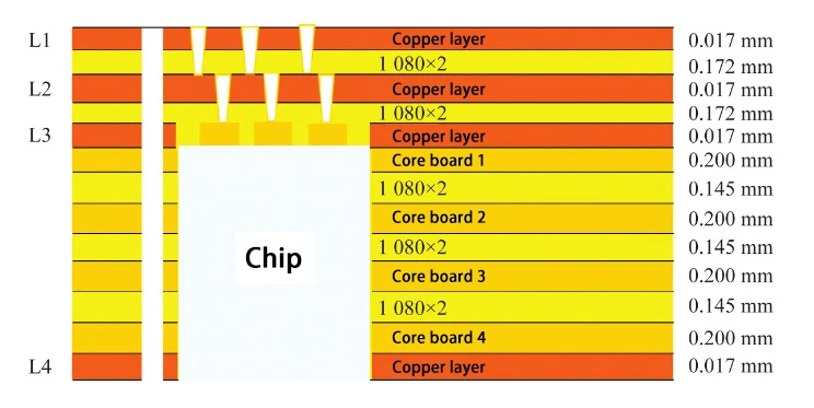
The structure of a 4-layers, Tier II, high-density interconnect (HDI) PCB is shown as below:
1.2 Analysis of Manufacturing Difficulties
(1) As shown in Figure 1, this HDI PCB has an asymmetrical structure with two single-sided blind vias. The manufacturing process requires laminations for twice: the first lamination embeds the chip within layers L3-L4, on the core board and laminates it with layer L2, completing the L2-L4 lamination; subsequently, blind vias L2-L3 and layer L2 circuitry are fabricated, followed by a second lamination to laminate layers L1-L2.
Due to the asymmetrical stack-up structure, the PCB is prone to bending after fabrication. Optimizing the lamination structure to ensure sufficient bending resistance is one of the key point for this PCB. (Board bending should be controlled within 0.65-1.52mm).
(2) The thickness of dielectric layer of this PCB is 0.172mm and the via diameter is 0.2mm. Compare to common requirements of the dielectric layer is 0.075 mm and via diameter 0.1mm, both are significantly larger.
Therefore, a high-energy laser drilling machine should be applied for laser processing of blind vias. Furthermore, a dedicated electroplating filling process for blind vias needs to be considered and applied.
(3) The chip is located on the surface of L4 and requires copper plating, electroplating, or horizontal line immersion processes during fabrication. If the resin filling between the chip and the substrate is insufficient during lamination, gaps or voids may exist, allowing chemicals to seep into these gaps and corrode the chip. Avoiding residual voids or air bubbles during lamination is a key point in the lamination process.
This structure requires special control over the resin flow during lamination and the resin filling effect between the chip and the substrate after lamination, ensuring 100% void-free lamination.
(4) Structurally, one side of the chip is bonded to the 1080 prepreg (PP) of layers L2-L3. Therefore, the surface treatment of the chip before the first lamination is crucial for improving adhesion.
Before lamination, the chip needs to going through surface-browning treatment, to increase surface roughness, to enhance adhension force. Due to the small chip size, the fan in the browning drying section must be turned off, or cease any air-flowing/winds, to prevent that the chip from being blown away. After browning, it needs to remove mositure, 120 ℃/1h, in static baking oven.
(5) The package material of this chip is ceramic, which has a low coefficient of thermal expansion. The chip is embedded inside the PCB, and the coefficient of thermal expansion of the PCB material must be close to the chip, which ensures the compatibility. Therefore, one of the key consideration is selecting the ideal PCB material.
1.3 Selection of PCB Structure Material
Analysis for the manufacturing difficulties has shown that when selecting materials for this board, factors such as board bending improvement, resin filling, and coefficient of thermal expansion must be considered.
Research on material selection for asymmetrical structural boards shows that the thinner the fiberglass used in PP fabrication, the better it improves the anti-bending performance.
For this board, both the laminated PP and the core require thin fiberglass PP. The 0.2mm core requires lamination with 3313×2 PP, using 1080 PP (high resin content, 68%). Furthermore, selecting materials with a low coefficient of thermal expansion and high Tg would result in better dimensional stability (selecting materials with Tg ≥ 190 ℃).
2. Manufacturing Process
Given the structural characteristics of the 4-layers, Tier II, HDI board with embedded chip, traditional common PCB manufacturing processes need adjustments and optimizations. The process must consider the accuracy of chip placement, capacity of resin filling, the processing quality of micro-blind via, and dimensional stability of post-lamination, to ensure the final product meets the requirements of high-density interconnection with high reliability. The key processes will be described in steps below.
2.1 Core Fabrication
As shown in Figure 1, there are 1, 2, 3, and 4 cores. Core 1 only carries the circuits on layer L3, with no copper foils on the other side. After etching, targeted holes will be punched. Core 2 and 3 have no circuits as well, targeted holes will be punched. Core 4 has all-copper circuits for layer L4, without copper on the other side. After etching, target holes will be punched.
2.2 Core Milling and PP Milling
A CNC milling machine, require milling accuracy within ±0.050mm will be applied for milling, creating a groove which leave a space of 0.075mm from each side of the chip. The same method will be used to mill a groove on the PP, 0.125 mm space on each side of the chip. It is better to mill in a clean room or specific environment, as the PP needs to be stored in an environment with stable temperature and humidity, to meet the clean standards and ensure good lamination quality.
2.3 First Lamination
After the first lamination, the PCB thickness ranges from 1.35 to 1.65 mm.
(1) Browning of cores 1, 2, 3, 4: The chips need to be browned by fixtures. During this process, blower, fan or any equipment could flow the air, should be turned off when the chips going through the drying section. After browning, bake in oven at 120 ℃, for 1 hour.
(2) In order to prevent the cores from sliding and chip misalignment during lamination, the alignment deviation of the cores must be within 0.075 mm. Positioning is achieved using pinning lamination (PIN LAM). If PIN LAM lamination equipment is unavailable, the core boards must be fixed by rivets, to enhance the positioning.
(3) When stacking boards, the gel-resisting film must be stacked on the steel plate first: If press by PIN LAM, the resist film must be punched first for positioning, and the PP must also be punched; If using rivets positioning, place the core board that has been riveted on the resist film. Placing the chip into the slot, stack 1080×2 PP between L2 and L3, cover with layer L2 copper foil, and finally cover with a steel plate, stacking a total of 10 layers.
(4) The parameters of lamination are crucial
After the lamination of high-temperature, the pressure of the cooling section should be set at 10 kg/cm² or below, to cool down the PCB slowly with low pressure. Another key point is to ensure sufficient resin filling gaps around the chip, selecting 1080 PP with a resin content of 68%.
During the lamination process, when the material temperature is in the range of 80~120℃, the heating rate needs to be increased (3.5 ℃/min; the higher the heating rate, the better the resin flowability and filling properties), and a higher transfer point pressure (32 kg/cm²) should be set on.
2.4 Post-Lamination Processing
(1) Grind the board edges and drill positioning holes.
Drill the positioning holes of the PCB by X-ray drilling machine and process the board edges with cutting&grinding machines.
(2) Remove residual resin on the chip surface by lasering, ensuring the duty cycle as 90%.
(3) Remove adhesive residue from the board surface and transport to the copper plating process, to remove residual resin from the PCB copper surface.
(4) Inspect the chip flatness by 3D measuring instrument, the flatness of the chip with board surface should be −10~+20μm.
2.5 L2: Laser Drilling for Blind Holes
(1) Drill positioning holes, expose with a special photopolymer dry film, going through acid etching process and etch out the opennings of blind hole positions.
(2) Drill the blind holes on the L2 surface by laser, make the hole diameter as 0.2mm. (The laser drilling machine is from Mitsubishi.)
2.6 L2: Blind Hole Metallization
(1) After laser drilling, remove residual adhesive inside the blind holes.
(2) Chemical cleaning of the blind vias. Set the water pressure to the upper limit.
(3) Inspect the bottom of the L2 blind vias, by professional AOI, to confirm there is no resin residue inside.
(4) Baking the board at 200℃ for 2 hours before chemical copper plating;
(5) Complete the chemical copper plating on a horizontal copper plating line.
2.7 L2: Through-hole Plating
(1) During the first through-hole plating, no current is passed through the non-blind via surfaces. The minimum copper thickness for blind vias is 15μm, and the copper thickness on the board surface is 75~95μm.
(2) Prepare a dry film for the plating. Complete the preparation during the outer layer circuit process, retaining the blind vias and covering the entire board surface with the film for the non-blind vias.
(3) For the second through-hole plating, only plating the vias, not the board surface, ensuring 100% filling of the blind vias.
(4) Remove the film: Remove the dry film from the board surface along the removal line.
(5) During the grinding process, only turn on the L2 surface grinding brush; do not turn it on on the L4 surface. The copper thickness after grinding should be controlled at 65-85 μm, with copper-filled via depressions ≤20 μm and protrusions ≤25 μm.
(6) Complete electroplating on the board surface. The minimum copper thickness on the L2 surface should be controlled at 105 μm, and no current should be passed through the L4 surface.
2.8 L2: Circuits
(1) Use photoresist dry film on the L2 layer and perform pattern transfer, by laser direct imaging (LDI). Apply a resist dry film to the L4 layer and expose in full.
(2) Etch the board along the acid etching line. Etch the circuit on the layer L2 and apply etching-resist film on the layer L4, to protect L4. After etching, remove the film.
(3) Inspect the circuits on layer L2, by AOI.
2.9 Second Lamination
(1) Before browning, bake the PCB at 120℃ for 2 hours, and after browning, bake it again at 120℃ for 2 hours.
(2) Pre-stack the PCB, placing 1080×2 PP sheets on layers L1~L2.
(3) Before stacking, place copper foil (with the rough surface of the copper foil in contact with the steel plate) or release film on the steel plate, then place the pre-stacked PCB with L4 facing down, and place 17μm copper foil on top of the 1080×2 PP sheets on layers L1~L2.
(4) Set the lamination pressure during the cooling stage to below 10kg/cm², to cooling down the PCB with low pressure, reducing the internal force slowly which was generated during lamination.
2.10 Post-Lamination Processing
(1) After lamination, drill the positioning holes by X-ray drill machine, then grind the edges.
(2) Transport PCB to the copper plating process for a desmearing process, to remove resin residuals from the copper surface.
2.11 L1 Copper Reduction
(1) Prepare the outer dry film, leaving the layer L1 uncovered and the layer L4 covered.
(2) Reduce the copper thickness of the layer L1 to 7~9μm on the copper reduction line.
(3) Remove the film completely from the layer L4.
2.12 L1 Laser Drilling
(1) Expose the blind holes on the L1 surface by a photopolymer dry film with opennings, and fully expose the L4 surface to create a resist dry film.
(2) Acid etching to create blind vias on the L1 surface for positioning and opening, followed by film removal.
(3) Laser drilling of blind vias: Drilling holes with a diameter of 0.2mm from the L1 surface, by a Mitsubishi laser drilling machine.
2.13 Metallization of L1 Blind Vias
(1) After laser drilling, plasma desmearing.
(2) Chemical cleaning of the blind vias.
(3) Inspection of the L1 blind vias through AOI, focusing on the resin residues at the bottom of the blind vias.
(4) Baking the board at 200℃ for 2 hours before chemical copper plating, then fabricating the board on the horizontal copper plating line.
2.14 L1 Hole Filling Electroplating
(1) After the first time of hole electroplating, the minimum copper thickness of blind holes is 15μm, the copper thickness on the board surface is 50~70μm, and no current is passed through the L4 surface.
(2) After the first time of hole electroplating, a dry film is applied to the L1 surface, retaining the blind hole positions, and the entire L4 surface is covered with a dry film.
(3) For the second hole electroplating, only the holes are plated, and no current is passed through the L4 surface.
(4) The dry film on the board surface is removed.
(5) When going through grinding process, only the grinding brush on the L1 surface is turned on, and the brush on the L4 surface is not turned on. The copper thickness after grinding is controlled at 40~60μm, the copper hole filling depression is ≤20μm, and the protrusion is ≤25μm.
2.15 Through-Hole Fabrication
(1) Through-holes fabricated by mechanical drilling.
(2) Before copper plating, the board will be baked at 200℃ for 2 hours.
(3) Through-hole chemical copper plating.
(4) Board surface electroplating: After the board is grinded, surface electroplating is finished, L1 is electroplated, and no current is passed through the L4 panel.
2.16 Outer layer circuit fabrication
(1) Use dedicated circuit data, photoresist dry film, and LDI exposure machine for production.
(2) Etch the board by acid. The layer L1 carries the circuits, and the layer L4 has no circuit.
(3) Inspect the outer layer circuits by AOI.
2.17 Solder resist and post-processing
(1) Solder resist applied by normal processes: grinding, screen printing, low-temperature baking, exposure, development and high-temperature baking; copper is exposed at the layer L4 chip position, and solder resist is fully applied to other positions.
(2) The surface treatment for this board is chemical gold plating, normal processes.
(3) Use a CNC milling machine to complete the forming process.
(4) Test the circuits;
(5) Use a dedicated board bending and pressing oven for pressing, at 150℃ for 4 hours, followed by 100% board bending testing (board bending should be controlled within 0.65mm/1.52mm).
(6) Finally, inspect the quality of board surface by automated visual inspection (AVI) equipment.
After the quality inspection department confirms the board is qualified, it is ready for package and shipment.
3. Quality Analysis of Key Processes
To ensure that the 4-layers, tier II, embedded chip HDI board is stable and reliable, the performance of electrical, high-density interconnect and embedded structure, it is necessary to verify the quality of key processes and the final product systematically.
The quality analysis includes:
- The deformation of the board after lamination and processing.
- The flatness of the embedded chip area.
- The potential void defects that may occur inside the micro-blind vias and resin-filled structures.
Through measurement, slicing, and comparison, process compatibility can be assessed promptly, providing a basis for process optimization.
3.1 Bending Data
After completing the bending process, 50 boards had been picked out randomly as samples for statistics. The required bending rate was within 0.65mm/1.52mm, the measured data on samples were 0.53~0.63mm/1.41~1.51mm, the results are positive and meet requirements.
The measurement data shows that although the structure is asymmetrical, the overall bending performance is good.
3.2 Chip Flatness Data
After lamination, the chip flatness range is required to be -10 to +20 μm (concave/convex). After removing adhesive residue, the locations of 50 chips were picked out for measurement. The concave/convexity data ranged from -1.0 to -8.0 μm. After this lamination, the chip flatness data were all within the required ranges.
3.3 Cross-Inspection for Voids
Twenty chips were picked out as samples for cross-inspection, after lamination, to observe the voids between chips and the substrates. No voids were found in any of the 20 samples. It indicates that high-resin-content 1080 PP was used during lamination, and the core board was milled by high-precision CNC milling machine, controlling the groove width, within 0.075μm on each side, ensured resin filling effectively.
3.4 Reflow Soldering Reliability
5 samples were picked out randomly for reflow soldering, at 270℃ for 3 times. The cross-inspect to observe the separation between chips and substrate. The results shown there was no separation between the chip and the substrate, and no failure at the chip and blind via connections.
4. Conclusion
Through process monitoring, board bending data, chip flatness, and reflow soldering reliability assessment, the results were confirmed that all meets customer's requirements and acceptable standards, verifying the quality and feasibility.
Benlida has been manufacturing PCB for 14 years, with years of experience and professional-oriented upgrading, rigorous process management and quality control, nowadays Benlida manufacture HDI PCB for many customers, from domestic to global markets. If you need HDI PCB or encounted relative issues, please contact Benlida to know more!
 en
en


 WhatsApp