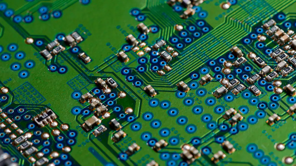
Via-in-pad lets you put microvias right under where parts sit. This helps you use all the space on the PCB, which is good for small BGA packages. You can place parts closer together and still keep signals clear. Bypass capacitors can go near power pins to cut down noise and make signals better. Important signals can move through layers right under the part. For fast signals, you keep the path short and do not need extra lines. Via-in-pad also helps move heat away from power parts by linking pads to copper planes.
1. Makes more room for small layouts
2. Keeps signals strong by using short paths
3. Helps cool down power parts
4. Let's you place tiny parts easily
Semi-Vertical Connections
Semi-vertical microvias make slanted paths between layers. These help you fit wires in tight spots and get around things in the way. They work well when the board has many layers in tricky patterns.
Note: Semi-vertical microvias give you more ways to route wires. You can use them to fix space problems and make signals better in advanced HDI multilayer PCBs.
Microvias let you join layers, save space, and make your board work better. You can pick the best type for your project and build strong, high-density boards.
Microvia Manufacturing and Laser Drilling
Laser Drilling Process
Laser drilling is used for HDI PCBs to make microvias very accurately. This way, you can make holes smaller than 50 micrometers. These holes are much smaller than what old methods could do. You can also control the shape of each microvia. For example, a microvia that is 100 microns wide and 80 microns deep has a good 0.8:1 ratio. This shape helps copper stick well and keeps connections strong. New laser drilling machines work with many different materials. They also lower heat damage, especially with femtosecond lasers. Production is faster and costs less. Automated laser drilling for HDI PCBs can make things over 50% faster and cut costs by up to 35%.
1. Laser drilling for HDI PCBs gives you:
2. Very small via holes under 50 μm
3. Faster work and lower costs
4. Works with new dielectric and via-fill materials
One-Step Blind Via Formation
You can make blind microvias in just one step. This makes lamination much easier. It can cut down lamination steps by up to 60%. You save time and lower the chance of mistakes. One-step blind via formation also lines up layers better. Your microvias connect right where you want them. Using the right tools and materials helps you avoid heat damage and alignment problems.
Tip: Always check the aspect ratio and pick materials that fit well. This keeps your microvias working right.
Quality Control and Inspection
Quality control is key when making microvias. You need special tools to find problems early. X-ray inspection lets you look inside the board. You can spot voids, dimples, or bad copper fill. Thermal cycling tests check if microvias can handle hot and cold without breaking. Here are some common problems and how to stop them:
| Defect Type | Description | Mitigation Strategy |
|---|
| Interfacial Separation | Microvia base comes off the pad due to heat stress | Use matching materials and set soldering right |
| Barrel Cracks | Cracks in copper from heat or force | Test with heat cycles and design for even stress |
| Voids and Dimples | Not enough copper plating | Plate better and check carefully |
You keep microvias strong and safe by following these steps and using the best checks.
Benefits, Reliability, and Cost in High-Density Interconnect
Increased Routing Density
Microvias let you fit more connections in less space. You can build smaller boards with more features. Traces can be closer together. This makes more channels for signals. You can reach up to 100 vias in one square centimeter. This is much more than old boards. You can use thinner traces and spacing. This helps your board work better and keeps signals clear.
| Layout Parameter | Typical Values | Impact on Performance |
|---|
| Trace Width | 50 µm or finer | Controls impedance, reduces crosstalk |
| Trace Spacing | 50 µm or finer | Prevents shorts, controls coupling |
| Via-in-Pad Diameter | 100 – 150 µm | Saves PCB real estate, shortens signal path |
Microvias help you add more I/O channels. Your design becomes more flexible. You can send fast signals with less interference. Microvias give you big benefits for advanced pcb designs.
Performance and Space Efficiency
Microvias give you many advantages in HDI multilayer PCBs. You can use smaller vias and thinner traces. This lets you fit more features on your board. You save space and make routing easier. Microvias also make signals travel shorter paths. This means faster signals and less loss.
1. More routing density gives you extra trace channels and I/O breakouts.
2. Shorter interconnects and copper-filled microvias keep signals strong.
3. Microvias are smaller than old vias, so you save space.
4. HDI multilayer PCBs use thinner traces for more connections.
5. You can reach up to 100 vias per square centimeter.
6. The HDI PCB multilayer structure makes signals travel shorter paths.
Microvias help you build boards that work well for high-performance jobs. You can control impedance and keep signals strong. This makes your design better.
Reliability Challenges and Solutions
You must think about reliability when using microvias in HDI PCBs. Microvias face problems like stress and material defects. Copper and dielectric materials grow at different rates. This can cause cracks or holes. Bad process control can make the plating too thin. Stacking more than two microvias or putting microvias on buried vias can cause trouble.
| Aspect | Traditional Vias | Microvias |
|---|
| Diameter | 150µm–500µm | Smaller diameter, typically less than 100µm |
| Aspect Ratio | High aspect ratios lead to uneven plating | Lower aspect ratios improve reliability |
| Reliability Risks | Prone to cracking, void formation, and thermal cycling failures | Designed to mitigate these issues, but still have specific failure modes |
| Thermal Cycling | Rigid structures prone to cracking | More resilient, but voids can lead to failures |
| Mechanical Shock | Vulnerable to premature failure | Better performance, but voids can still be problematic |
You can fix these problems by staggering microvias and not stacking too many. Pick materials that handle heat well. Use strict process controls and test for reliability. These steps make your boards safer and stronger.
Tip: Always test microvias with heat and stress tests. This helps you find weak spots early and fix them.
Cost Optimization Strategies
You can save money when building HDI multilayer PCBs with microvias. HDI boards cost more than standard boards. Careful planning helps you spend less.
| Microvia Type | Cost Implication |
|---|
| Stacked Microvias | Higher costs due to complexity in alignment and filling |
| Staggered Microvias | Lower costs due to simplified manufacturing processes |
HDI boards can cost two to five times more than standard boards. A regular 4-layer PCB costs about $0.50 per square inch. An HDI board with via-in-pad can cost $1.50 to $3.00 per square inch.
You can use these ways to save money:
1. Make your design simple. Use fewer layers and avoid tight tolerances.
2. Pick cheaper materials. Use standard materials like FR-4 for less important jobs.
3. Plan for efficient panelization. Fit more boards on each panel.
4. Limit complex features. Only use blind or buried vias and microvias if needed.
These steps help you balance performance and cost in your PCB design.
Design Tips for HDI Multilayer PCBs
You can get the best results from microvias by following smart tips. Plan your stack-up early. Decide the number of layers and via types at the start. This stops expensive changes and keeps your board balanced.
Place vias carefully. Use blind and buried vias inside to save surface space and lower signal interference.
Control impedance. Match trace widths and materials to keep impedance steady, usually around 50 ohms for fast signals.
Work with manufacturers. Learn their skills for microvia drilling and layer stacking. Set tolerances clearly.
Test for reliability. Use heat and stress tests to check stacked vias.
1. Plan your stack-up early. Make a balanced board to stop warping.
2. Place stacked vias wisely. Avoid crowding and make routing easy.
3. Work with manufacturers. Make sure they can handle tight tolerances, like via aspect ratios below 0.75:1.
4. reliability test. Check stacked vias for strength in your design.
Microvias let you build boards with high routing density, strong integrity, and reliable performance. You can scale your design for modern electronics. You get the benefits of microvias and make your hdi pcb multilayer structure ready for fast signals and high-performance jobs.
Microvia technology helps you make HDI multilayer PCBs smaller and faster. These boards also become more reliable. You get better density, signal quality, and easier manufacturing:
| Feature | Microvia Advantage |
|---|
| Density | 50% more connections in less space |
| Signal Performance | Faster signals, lower attenuation |
| Reliability | Less than 2% failure after 1,000 cycles |
| Manufacturing Yield | Up to 98% success rate |
You do well by knowing microvia types and design rules. Using DFM guidelines helps too. You can fit more connections in small areas. This means fewer mistakes and lower costs.
Microvias are used in advanced electronics, like medical devices. They are also used in microwave PCBs. In five years, microvias will likely be standard. This will help you keep up with new needs in many industries.
FAQ
What makes microvias important in HDI PCB design?
Microvias help you build HDI boards with more layers and a smaller size. You can fit more parts and connections. This lets you create advanced hdi devices that work faster and use less space.
How do you choose the right microvia type for HDI multilayer PCBs?
You pick microvia types based on your HDI board needs. Blind microvias connect the surface to the inner layers. Buried microvias link inner layers. Stacked microvias reach deeper. Via-in-pad helps with heat and signal paths in HDI designs.
Can microvias improve signal quality in HDI PCBs?
Microvias make signal paths shorter in HDI boards. You get less loss and better performance. Your HDI design sends fast signals with less interference. This helps your hdi PCB work well in high-speed jobs.
What are common reliability issues with microvias in HDI boards?
You may see cracks, voids, or separation in HDI microvias. These problems happen from heat or stress. You fix them by using strong materials and testing your hdi PCB for reliability.
How can you lower costs when designing HDI multilayer PCBs with microvias?
You save money by planning your HDI layout early. Use fewer layers and simple microvia types. Choose standard materials for your hdi board. Work with your manufacturer to avoid mistakes and keep your HDI PCB cost low.
Tip: Always check your hdi PCB for defects before production. This helps you avoid costly errors.
| Microvia Type | Best Use in HDI PCB |
|---|
| Blind | Surface to inner layer |
| Buried | Inner layer to inner layer |
| Stacked | Deep connections |
| Via-in-pad | Heat and signal management |
As a major in Electronics and Mechanical Automation, Sonic has been engaged in PCB design, R&D, and manufacturing of electronics for around 22 years, as the engineering director, and coordinates with the supply chain(components and CNC parts), providing professional support and consulting for global customers.
 en
en


 WhatsApp