PCB surface treatment is a critical layer which connect components to PCB solder pads, directly affecting solderability, reliability, and cost. Here is the detailed comparison of most common-applied surface treatment types:
.webp)
Core Comparison Overview:
| Type | Full Name | Advantages | Disadvantages | Applications |
| HASL | Hot Air Leveling | Low cost, good solderability, long shelf life, reworkable | Uneven surface, not suitable for fine pitch, thermal shock | Consumer electronics, computer boards, low-density boards |
| ENIG | Chemical Plating Nickel Gold | Flat surface, good solderability, suitable for wire bonding, oxidation resistant | High cost, potential "black disk" risk, complex manufacturing process | BGA, QFN, connectors, high-frequency boards, button positions |
| OSP | Organic Solder Protector | Extremely low cost, flat surface, process is simple and environmentally friendly | Short shelf life, not resistant to repeated reflow-soldering, difficult to detect | High-volume consumer electronics (such as mobile phone, TV motherboards) |
| Immersion Tin | Chemical Plating | Flat surface, suitable for fine pitch, moderate cost | Prone to solder whiskers, relatively short shelf life, susceptible to scratches | Fine pitch SMT, automotive electronics (partial) |
| Immersion Silver | Chemical Plating Silver | Flat surface, excellent electrical properties, moderate cost | Prone to sulfidation and yellowing, average shelf life, susceptible to contamination | High-speed digital circuits, RF microwaves, LEDs |
| ENEPIG | Chemical Nickel-Palladium-Gold | No black disk risk, suitable for gold/aluminum wire bonding, extremely high reliability | Highest cost, most complex process | High reliability for military and aerospace applications, chip-level packaging. |
Detailed Overview of Each Option:
1. HASL (Hot Air Leveling)
Manufacturing Process: The PCB is immersed in molten solder (usually tin-lead or lead-free tin), then blow away the excess solder by hot air.
Advantages:
● Lowest cost, most mature process.
● Excellent at soldering performance and compatibility, the solder itself is the soldering material.
● Long shelf life (usually 12 months), applicable for rework&repair.
Disadvantages:
● Uneven surface: For fine-pitch BGA and QFP components, it may cause short circuits or tombstoning.
● Thermal shock: The high-temperature process may have stress effects on the board material.
● Environmental issues: Lead-free HASL has a higher temperature (approximately 260°C), resulting in higher energy consumption.
Summary: While considered an "economical choice," it's being replaced by flatter processes, but remains mainstream in the low-to-mid-range market.
2. ENIG (Electrochemical Electroless Nickel-Gold)
Manufacturing Process: A layer of nickel chemically deposited on copper surface (as a barrier and solderable layer), then covered by a thin layer of gold (for oxidation prevention).
Advantages:
● Extremely flat surface, suitable for high-density, fine-pitch components (such as BGAs).
● The gold layer is oxidation-resistant and has a long shelf life (typically 12 months).
● The nickel layer is hard and wear-resistant; the gold surface is suitable for gold wire bonding and contact interfaces (such as gold fingers).
Disadvantages:
● High cost (second only to ENEPIG).
● Risk of "black pad": Excessive corrosion between the nickel and gold layers could lead to abnormal phosphorus content, causing brittle fracture of the solder, a fatal defect. Now this processes could be well controlled due to management.
Summary: A "mainstream choice for high-end electronics," widely used in applications which require flat surface and high reliability.
3. OSP (Organic Solder Protector)
Manufacturing Process: A water-soluble organic compound (usually azoles) is coated onto a clean copper surface to protect it from oxidation.
Advantages:
● Extremely low cost, environmentally friendly (no metal pollution).
● Absolutely flat surface.
● High solder joint strength.
Disadvantages:
● Short shelf life (typically 3-6 months), requires strict storage conditions.
● The film is transparent and difficult to detect.
● Not resistant to repeated thermal cycles (generally recommended ≤2 reflow soldering cycles).
● Not suitable for press-fit technology or as a contact interface.
Summary: A "low-cost, high-performance & invisible shield," favored for high-volume, fast-turnover consumer electronics, but requires high-level supply chain management.
4. Chemical Tin Deposition
Manufacturing Process: A layer of pure tin is deposited on the copper surface through a displacement reaction.
Advantages:
● Flat surface, suitable for fine pitch.
● Compatible with all soldering processes.
● Cost between OSP and ENIG.
Disadvantages:
● Temperature:
1) Tin whiskers may grow under prolonged temperature and humidity changes, posing a short-circuit risk. This is a significant concern for high-reliability products.
2) The tin layer is relatively soft and easily scratched.
● Shelf life: Generally short (usually 6 months).
Summary: The risk of tin whiskers needs to be assessed carefully, it is widely applied in consumer electronics and some automotive sectors.
5. Immersion Silver
Manufacturing Process: A thin layer of silver is deposited on a copper surface through a displacement reaction.
Advantages:
● Smooth surface, excellent conductivity, ideal for high-frequency, high-speed signals.
● Good solderability, high solder joint strength.
● Cost comparable to immersion tin.
Disadvantages:
● Temperature: Prone to sulfidation or oxidation: Exposure to sulfur-containing environments will cause yellowing or blackening, which does not affect solderability but impacts appearance and acceptance.
● Susceptible to chloride ion contamination.
● Slight risk of silver migration (under high-voltage, humid environments).**
Summary: A "good friend to signal integrity," widely used in RF, microwave, and high-speed digital circuits.
6. ENEPIG (Chemical Nickel-Palladium-Gold)
Manufacturing Process: A thin palladium layer is added between the nickel and gold layers (EPIG: Chemical Impregnation Palladium Gold is a simplified version).
Advantages:
● Completely eliminates the risk of "black disk" corrosion: The palladium layer effectively prevents excessive nickel corrosion.
● Suitable for both gold and aluminum wire bonding, resulting in higher bond strength.
● Highest reliability of all surface treatments.
Disadvantages:
● Highest cost (due to the use of the precious metal palladium).
● Most complex process control.
Summary: "Luxury-level assurance," primarily used in chip-scale packaging, military aerospace, and medical fields with extremely stringent reliability requirements.
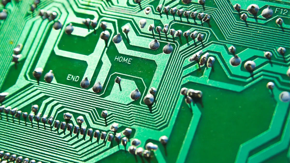
.webp)
Consideration for Choose:
Cost-priority, simple board design: Choose HASL or OSP.
High-density, fine-pitch SMT (e.g., BGA): Choose ENIG or Im-Ag.
Requires gold wire bonding or contact interfaces: Choose ENIG or ENEPIG.
For high-frequency, high-speed signals: Im-Ag is the preferred choice, followed by ENIG.
For extremely high reliability, regardless of cost: ENEPIG is the choice.
For those prioritizing environmental friendliness, solderability, and flatness: OSP offers the best cost-performance ratio.
Avoid solder whiskers: Use immersion solder with caution in the automotive and aerospace industries.
Benlida has focused on PCB manufacturing for 14 years, continuously upgrade equipment and processes, and a strong team has been cultivated. If you need PCB, please feel free to contact Benlida, we hope this detailed comparison could help you to understand PCB surface treatment processes and make the right choice!
 en
en


 WhatsApp