Power electronics used in new energy charging equipment have changed significantly over the past decade. Whether the application is an AC wall charger, an on-board charger (OBC), a DC fast charging station, or an energy storage converter, engineers are being asked to deliver higher output power within increasingly compact enclosures. At the same time, charging efficiency, long-term reliability, electromagnetic compatibility, and thermal performance have become equally important design targets.
These requirements place considerable pressure on the printed circuit board. While semiconductor technologies such as SiC MOSFETs and GaN devices continue to improve switching efficiency, the PCB that supports these devices must also evolve. Traditional FR4 boards remain suitable for many low-power electronic products, but their thermal limitations become increasingly apparent as power density rises.
This is one of the main reasons New Energy Charger PCB Assembly is gradually shifting toward ceramic-based substrates in high-power applications. The discussion is no longer limited to selecting a PCB material with higher thermal conductivity. Instead, engineers evaluate the entire thermal path—from semiconductor junctions and copper layers to ceramic substrates, solder joints, and heat sinks—to improve overall system reliability.
Another important change is that PCB performance alone is no longer sufficient. Even a well-designed ceramic PCB may fail to achieve its expected lifespan if assembly processes are not carefully controlled. Component placement, solder voids, thermal pad quality, reflow temperature profiles, inspection procedures, and reliability testing all influence the final performance of a charger operating continuously under demanding electrical and environmental conditions.
For manufacturers developing EV chargers, industrial charging systems, renewable energy converters, and high-power power supplies, the discussion has therefore shifted from selecting a PCB to optimizing the entire Ceramic PCB Assembly process.
Why Ceramic PCB Is Replacing Conventional FR4 in High-Power Charger Designs
The PCB inside a modern charger performs far more than electrical interconnection. It also becomes an important part of the thermal management system.
Every power conversion stage generates heat. Switching devices, power inductors, transformers, rectifiers, and current sensing components continuously convert electrical energy while simultaneously producing thermal energy. If that heat cannot be transferred efficiently away from critical components, junction temperatures rise rapidly, reducing efficiency and accelerating component aging.
For conventional consumer electronics operating at relatively low power, FR4 remains an economical choice.
Its advantages include:
· Mature manufacturing technology
· Low production cost
· Good mechanical stability
· Broad supply chain availability
· Compatibility with standard SMT assembly
However, FR4 has one fundamental limitation.
Its thermal conductivity is only around 0.3 W/m·K.
As charging power increases from several hundred watts to tens or even hundreds of kilowatts, this level of thermal performance becomes increasingly inadequate.
Fast chargers for electric vehicles, industrial battery charging equipment, photovoltaic energy storage systems, and high-power DC/DC converters all generate localized heat around semiconductor devices.
When heat accumulates inside the PCB structure, engineers often observe several problems:
· Rising junction temperatures
· Reduced conversion efficiency
· Uneven thermal distribution
· Accelerated solder fatigue
· Shortened capacitor lifetime
· Increased cooling requirements
Rather than relying entirely on larger heat sinks or more powerful cooling fans, designers increasingly improve heat transfer directly at the PCB level.
Ceramic substrates provide a significantly more effective thermal pathway.
Compared with FR4, commonly used ceramic materials offer dramatically higher thermal conductivity.
PCB Material | Approximate Thermal Conductivity | Typical Applications |
FR4 | ~0.3 W/m·K | Consumer electronics, low-power control boards |
Alumina (Al₂O₃) | ~24 W/m·K | General power electronics, industrial power supplies |
Aluminum Nitride (AlN) | ~170 W/m·K | High-power EV chargers, SiC modules |
Silicon Nitride (Si₃N₄) | ~220 W/m·K | Automotive power electronics, high-reliability systems |
The difference is substantial.
Instead of allowing heat to remain concentrated around MOSFETs or IGBTs, ceramic substrates rapidly conduct thermal energy toward the cooling structure, reducing thermal resistance throughout the power module.
This lower operating temperature produces several practical benefits.
· Improved semiconductor efficiency
· Lower thermal stress
· Reduced cooling system requirements
· Higher continuous output capability
· Longer component service life
For EV Charger PCB applications operating around the clock, these improvements directly influence maintenance intervals and long-term operating costs.
Comparing Ceramic PCB Materials for New Energy Electronics
Although ceramic PCBs are often discussed as a single technology, several ceramic materials are available, each optimized for different engineering priorities.
Material selection depends on balancing thermal performance, mechanical reliability, manufacturing complexity, and project cost.
Alumina PCB
Alumina remains the most widely used ceramic substrate because it offers stable electrical insulation, mature manufacturing processes, and relatively economical production costs.
Typical characteristics include:
· Stable electrical performance
· Good mechanical rigidity
· Reliable dimensional stability
· Mature metallization technology
· Competitive manufacturing cost
Because of these characteristics, Alumina PCBs are commonly used in:
· Industrial power supplies
· Motor controllers
· LED drivers
· Medium-power charging equipment
· Industrial control electronics
For many charger manufacturers, Alumina provides an effective balance between performance and production cost.
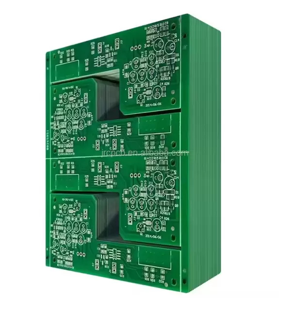
Aluminum Nitride PCB
As charging power continues to increase, Aluminum Nitride becomes increasingly attractive.
Its thermal conductivity approaches that of some metals while maintaining excellent electrical insulation.
Key engineering advantages include:
· Outstanding heat conduction
· Low coefficient of thermal expansion
· Excellent electrical insulation
· Compatibility with high-power semiconductor packages
· Stable performance under elevated temperatures
These characteristics make AlN particularly suitable for:
· SiC MOSFET modules
· High-power DC fast chargers
· EV onboard chargers
· High-current DC/DC converters
· Industrial power conversion equipment
The low CTE also reduces mechanical stress between semiconductor packages and the substrate during repeated thermal cycling.
Silicon Nitride PCB
Silicon Nitride emphasizes mechanical durability.
Although engineers frequently focus on thermal conductivity, mechanical reliability is equally important in transportation applications where vibration, shock, and repeated thermal expansion occur throughout the equipment's lifetime.
Typical benefits include:
· High fracture toughness
· Excellent bending strength
· Superior crack resistance
· Long fatigue life
· Outstanding thermal shock resistance
Because of these characteristics, Silicon Nitride is often selected for:
· Automotive electronics
· Rail transportation
· Aerospace electronics
· High-vibration industrial equipment
· Mission-critical power electronics
Property | Alumina | Aluminum Nitride | Silicon Nitride |
Cost | Low | High | High |
Thermal Conductivity | Good | Excellent | Excellent |
Mechanical Strength | Good | Good | Outstanding |
Thermal Shock Resistance | Moderate | High | Very High |
Typical Applications | General power electronics | High-power chargers | Automotive & high-reliability systems |
Rather than asking which ceramic material is "better," engineers normally determine which substrate best matches the electrical, thermal, and mechanical requirements of a specific charging system.
A commercial AC charger, a 350 kW DC charging station, and an onboard charger installed inside an electric vehicle all operate under different environmental conditions and therefore benefit from different ceramic technologies.
Why PCB Assembly Often Determines Final Reliability
Selecting a ceramic substrate is only one stage of the manufacturing process.
In practice, many field failures originate not from PCB material selection but from assembly quality.
For New Energy Charger PCB Assembly, every manufacturing process influences long-term reliability because power devices operate under continuous thermal cycling.
During every charging cycle, semiconductor junction temperatures rise and fall repeatedly.
These temperature changes create expansion and contraction throughout the assembly.
If solder joints contain excessive voids, if thermal pads are improperly wetted, or if component placement creates uneven heat distribution, mechanical stress accumulates over thousands of operating hours.
Eventually this may result in:
· Solder fatigue
· Copper separation
· Localized overheating
· Reduced heat transfer efficiency
· Premature device failure
For this reason, PCB Assembly Services for high-power electronics place much greater emphasis on process control than ordinary consumer electronics production.
Critical manufacturing controls typically include:
· Optimized SMT Assembly parameters for large thermal-mass components
· Accurate stencil aperture design to reduce solder void formation
· Controlled reflow temperature profiles for ceramic substrates
· X-ray inspection of hidden solder joints beneath power packages
· AOI inspection for placement accuracy
· Functional electrical testing before shipment
· Thermal cycling validation for reliability assessment
For high-current charger assemblies using SiC or GaN devices, these manufacturing details often have as much influence on field reliability as the PCB material itself.
The engineering objective is therefore not simply producing a ceramic PCB, but delivering a complete Ceramic PCB Assembly capable of maintaining electrical, thermal, and mechanical stability throughout years of continuous service.
Thermal Management Becomes the Core of High-Power Charger Design
As charging power continues to increase, thermal management has become one of the primary engineering challenges in power electronics. Efficiency improvements in modern semiconductor devices reduce power loss, but they do not eliminate heat generation. Even a converter operating at 97–98% efficiency still converts a significant amount of electrical energy into heat when delivering tens or hundreds of kilowatts.
Consider a DC fast charger delivering 150 kW at 97% efficiency. Approximately 4.5 kW of heat must still be dissipated continuously. Without an effective thermal path, localized temperatures can rise rapidly around power devices, eventually affecting switching performance, insulation materials, magnetic components, and solder joints.
This explains why thermal management is no longer viewed as a separate mechanical design task. It begins with PCB material selection and extends through the entire New Energy Charger PCB Assembly process.
The primary heat sources inside a charger typically include:
· MOSFETs
· IGBTs
· SiC MOSFET power modules
· GaN switching devices
· Rectifier bridges
· Current sensing components
· High-frequency transformers
Each component produces heat differently. High-current devices generate concentrated heat, while magnetic components often create broader thermal distribution across the PCB. Engineers therefore evaluate both localized hot spots and overall temperature balance during PCB layout.
An effective thermal path generally consists of several interconnected layers:
Semiconductor Junction → Solder Layer → Copper Pad → Ceramic Substrate → Heat Spreader → Heat Sink → Cooling Air or Liquid
Every interface contributes thermal resistance. Improving only one section rarely solves the overall problem. Ceramic substrates reduce one of the largest bottlenecks by allowing heat to spread much more efficiently before it reaches the cooling structure.
Copper design also plays an important role.
Increasing copper thickness improves current carrying capability while enlarging the heat spreading area. However, excessive copper thickness introduces new manufacturing challenges, including more difficult reflow soldering and greater thermal stress during assembly.
Via structures deserve equal attention.
Properly designed thermal vias transfer heat from surface-mounted power devices to lower copper layers or dedicated cooling plates. Poorly positioned vias, insufficient quantities, or inadequate filling techniques reduce thermal performance considerably.
Engineers frequently compare several PCB technologies when designing high-power charging equipment.
PCB Technology | Thermal Performance | Typical Power Level | Typical Applications |
FR4 PCB | Low | Low to medium | Consumer electronics, control boards |
IMS PCB | Moderate | Medium | LED lighting, industrial drivers |
DBC Ceramic PCB | Excellent | High | EV chargers, IGBT modules |
Ceramic PCB | Excellent | High | High-frequency power conversion, power electronics |
Rather than replacing every FR4 board inside a charger, designers usually reserve ceramic substrates for the most thermally demanding sections, while control circuits continue using conventional multilayer FR4. This hybrid approach balances manufacturing cost with thermal performance.
High-Frequency Switching Places New Demands on PCB Design
Another reason ceramic technology is becoming increasingly common is the rapid increase in switching frequency.
Power conversion equipment has moved far beyond traditional low-frequency switching designs. Modern converters increasingly operate at frequencies such as:
· 100 kHz
· 300 kHz
· 500 kHz
· Several hundred kilohertz for SiC converters
· MHz-level switching in certain GaN applications
Higher switching frequencies reduce transformer size, improve power density, and increase charging efficiency. However, they also create new challenges for PCB design.
Signal integrity becomes more difficult to maintain.
Parasitic inductance and capacitance that were insignificant at lower frequencies begin affecting switching waveforms, voltage overshoot, ringing, and electromagnetic emissions.
Ceramic substrates offer several advantages under these operating conditions.
Their dielectric characteristics remain stable over a wide temperature range while exhibiting relatively low dielectric loss. Stable dielectric properties contribute to more predictable impedance control and improved switching behavior.
Layout optimization becomes equally important.
For high-frequency Power Electronics PCB designs, engineers typically focus on:
· Minimizing high-current loop areas
· Shortening switching paths
· Reducing parasitic inductance
· Separating power and control circuits
· Improving ground return paths
· Optimizing decoupling capacitor placement
These layout practices reduce switching noise while improving EMI performance.
Ceramic substrates also help maintain dimensional stability during manufacturing, allowing tighter tolerance control on conductor spacing for high-frequency applications.
As semiconductor technologies continue moving toward faster switching devices, PCB materials and assembly techniques must evolve alongside them rather than remaining unchanged.
How PCB Assembly Influences Long-Term Reliability
Power electronics rarely fail because of one catastrophic event. In many cases, degradation occurs gradually over years of operation.
Every charging cycle exposes the PCB assembly to repeated heating and cooling.
These temperature fluctuations produce continuous mechanical expansion and contraction throughout the structure.
The challenge becomes even greater because different materials expand at different rates.
Engineers therefore pay close attention to the Coefficient of Thermal Expansion (CTE) of every major component, including:
· Ceramic substrate
· Copper layers
· Solder alloy
· Semiconductor package
· Base plate
· Heat sink
Poor compatibility between these materials accelerates mechanical fatigue.
Typical long-term failure mechanisms include:
· Solder fatigue
· Delamination
· Copper trace lifting
· Bond wire degradation
· Thermal interface deterioration
· Ceramic cracking caused by excessive mechanical stress
A carefully controlled Ceramic PCB Assembly process minimizes these risks.
Reliability improvements often begin during DFM (Design for Manufacturability), long before production starts.
Engineers evaluate:
· Component spacing
· Thermal expansion compatibility
· Copper balancing
· Pad geometry
· Mechanical support
· Stress concentration areas
Manufacturing then adds another layer of quality control through optimized solder paste deposition, controlled reflow profiles, inspection procedures, and functional testing.
For automotive and industrial power electronics, production commonly includes:
· AOI inspection
· X-ray inspection
· ICT where applicable
· Functional testing
· Burn-in testing
· Thermal cycling validation
· Environmental stress screening
Rather than treating these processes as independent quality checks, manufacturers use them to verify that the completed New Energy Charger PCB Assembly can withstand continuous operation under demanding electrical and environmental conditions.
Typical Applications for Ceramic PCB Assembly
The advantages of ceramic substrates extend well beyond electric vehicle charging stations.
As power density increases across multiple industries, thermal management and long-term reliability become common engineering priorities.
Applications frequently adopting Ceramic PCB Assembly include:
· EV charging stations
· On-board chargers (OBC)
· DC/DC converters
· Battery Management Systems
· Energy Storage Systems (ESS)
· Solar inverters
· Wind power converters
· Industrial power supplies
· Telecom power equipment
· Medical imaging systems
· Rail transit electronics
· Industrial automation equipment
Although these systems operate in different industries, they share several technical characteristics.
They often run continuously, handle relatively high electrical loads, experience repeated thermal cycling, and require long service lives with minimal maintenance.
For this reason, engineers increasingly evaluate PCB materials and assembly quality together instead of considering them as separate purchasing decisions.
Manufacturing Process Control Matters as Much as Material Selection
Successful PCB Manufacturing for new energy electronics depends on maintaining consistency throughout production.
Several manufacturing stages directly influence reliability.
Typical process controls include:
· DFM verification before production
· Optimized PCB stack-up design
· Accurate stencil thickness selection
· Controlled solder paste volume
· Nitrogen reflow where required
· Selective soldering for mixed assemblies
· Cleaning processes compatible with power electronics
· Conformal coating for harsh environments
· Functional testing under electrical load
· Environmental reliability verification
Many manufacturers supplying automotive or industrial charging equipment also design production processes to satisfy IPC Class 2 or, where higher reliability is required, IPC Class 3 workmanship standards.
These standards do not guarantee product performance on their own, but they establish manufacturing requirements that support greater consistency across large production volumes.The transition toward ceramic substrates is being driven by practical engineering requirements rather than material trends alone. Higher charging power, increasing switching frequencies, compact equipment designs, and longer service life expectations all demand more effective thermal management and greater manufacturing consistency than conventional PCB technologies can often provide.
For modern New Energy Charger PCB Assembly, substrate selection and assembly quality are closely connected. Ceramic materials improve heat transfer, while carefully controlled SMT processes, thermal design, inspection procedures, and reliability validation determine whether those material advantages translate into dependable long-term performance.
As electric vehicles, renewable energy systems, industrial power supplies, and energy storage installations continue to expand, Ceramic PCB Assembly is expected to play an increasingly important role in supporting higher power density, improved thermal stability, and reliable operation throughout the service life of next-generation power electronics.
About the author:

Sonic Yang
As a major in Electronics and Mechanical Automation, Sonic has been engaged in PCB design, R&D, and manufacturing of electronics for around 22 years, as the engineering director, and coordinates with the supply chain(components and CNC parts), providing professional support and consulting for global customers.

 en
en

.webp)
 WhatsApp