WANG Xu, ZHANG Sheng-tao*, CHEN Shi-jin, GUO Hai-liang, LUO Jia-yu, WEN Ya-nan, GUO Mao-gui, XU Wei-lian
Abstract:
The filling of through holes on print circuit board (PCB) were carried out by copper electroplating in an acidic bath comprising 75 g/L CuSO4ꞏ5H2O, 230 g/L H2SO4, and some additives at temperature (22 ± 3) °C and current density 1.7 A/dm2 under air agitation. The effects of four types of additives including Cl−, polyethylene glycol (PEG-10000), 3,3′- dithiodipropane sulfonate (SPS), and 2,2′-dithiopyridine (2-PDS) on the hole filling were studied by evaluating the filling efficiency, dimple, copper coating thickness on the surface, and cross-sectional morphology of the filled through hole. The combination of additives was optimized as follows: Cl− 50-70 mg/L, PEG-10000 200-300 mg/L, SPS 8-11 mg/L, and 2-PDS 9-13 mg/L. The hole filling efficiency was up to 91.7% when electroplating with the optimized combination of additives. The copper coatings obtained were uniform, compact, and smooth, and had good resistance to thermal shock in temperature cycling and tin immersion tests, meeting the requirements of reliability for PCB application.
Keywords: print circuit board; through hole; copper electroplating; additive; filling efficiency; dimple; thickness of surface copper coating; reliability
As electronic products continue to evolve toward being “thinner, lighter, and smaller,” printed circuit boards (PCBs), as one of the key components in the electronics industry, are also undergoing continuous upgrading and optimization [1]. The conventional resin via-plugging process is complex, and subsequent issues are prone to occur, including insufficient filling in small-diameter vias, interconnection degradation caused by resin curing shrinkage, difficulty in eliminating voids inside the holes and residual resin on the board surface, and even via cracking resulting from mismatched coefficients of thermal expansion (CTE) between the filled resin and the laminate material [2–3]. In particular, for thin boards, once warpage or deformation occurs after resin planarization (sanding), it is difficult to recover. To shorten the PCB manufacturing flow, provide improved thermal conductivity, and achieve more reliable electrical interconnection, through-hole copper electroplating (via filling) has become one of the important technologies due to its superior performance, and it is of great significance for manufacturing next-generation advanced PCBs [4].
At present, the literature on through-hole copper electroplating via filling is relatively limited, and domestic via-filling technology is not yet mature; therefore, the market application of this technology remains relatively low.
Organic additives—namely accelerators, suppressors (inhibitors), and levelers—are indispensable components in the copper electroplating via-filling process. Common accelerators include bis(3-sulfopropyl) disulfide sodium salt (SPS) and 3-mercapto-1-propanesulfonate sodium salt (MPS) [5]; the suppressor is typically polyethylene glycol (PEG); and commonly used levelers include Janus Green B (JGB) [6], thiazolinyl dithiopropane sulfonate sodium salt (SH110) [7], nitrotetrazolium blue chloride (NTBC) [8], and other quaternary ammonium compounds. Each additive must be used in combination with other additives. In this work, a novel small-molecule organic compound, 2,2′-dipyridyl disulfide (2-PDS), was employed as the leveler; chloride ions were supplied by hydrochloric acid; SPS and PEG-10000 were used as the accelerator and suppressor, respectively; and a single-factor experimental method was applied to analyze the effects of various additives on through-hole via-filling performance, thereby obtaining their optimal concentration ranges.
1 Experimental
1.1 Main Reagents
Copper sulfate (99% CuSO₄·5H₂O), concentrated sulfuric acid (98% H₂SO₄), hydrochloric acid (36%–38% HCl), bis(3-sulfopropyl) disulfide sodium salt (SPS > 97%), polyethylene glycol (PEG-10000), and 2,2′-dipyridyl disulfide (2-PDS) were used.
All solutions were prepared with deionized water.
1.2 Preparation and Pretreatment of Test Panels
The base material was an IT158 panel with dimensions of 518 mm × 468 mm.
After panel cutting, drilling, cleaning, electroless copper deposition, and routing, test coupons of 60 mm × 130 mm were obtained, with a board thickness of approximately 180 μm and a hole diameter of 150 μm.
Before plating, the test coupons were subjected to alkaline degreasing [(45 ± 5) °C, 2–3 min], water rinsing, and acid dipping [(40 ± 10) mL/L concentrated sulfuric acid, 25 °C, 2–3 min].
1.3 Through-Hole Copper Electroplating
1.3.1 Via-Filling Mechanism
Unlike the “bottom-up” filling mode for blind vias, through-hole filling follows the “butterfly technique” [9–10]. As shown in Fig. 1a, the deposition rate of copper ions at the hole center is higher than that at the via entrance and the board surface, which promotes connection at the central region of the through hole, forming two blind-via-like cavities and resulting in a butterfly-shaped cross section. This mechanism can also be understood as the “adsorption → consumption → diffusion model” of organic additives [11]. Such “butterfly technique” filling avoids via mouth closure caused by poor mass transfer in the via-filling electrolyte, i.e., the “dog-bone” phenomenon (see Fig. 1b).
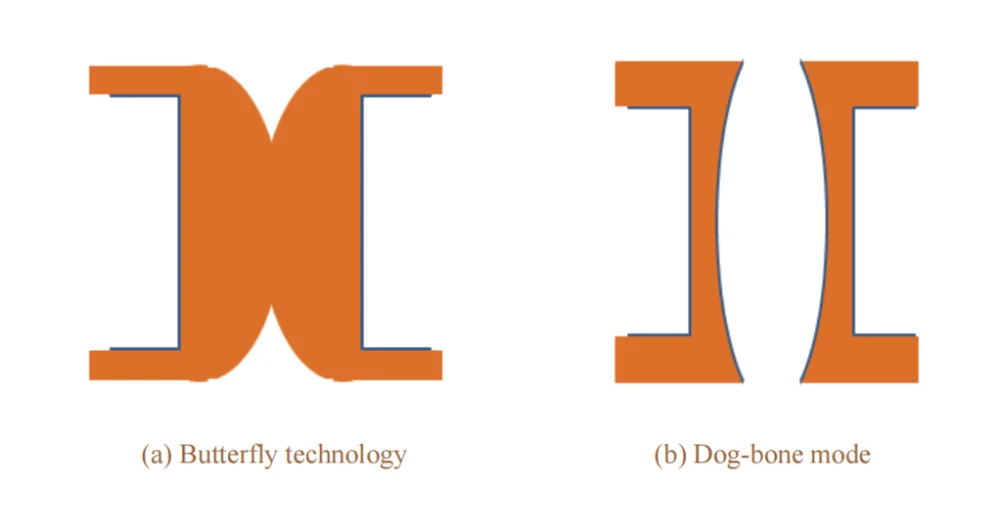
Figure 1 Filling mode of through hole by electroplating
1.3.2 Plating Bath Formulation and Process
A 1.5 L Haring cell was used. The test coupon was positioned at the center of the cell, and soluble phosphorized copper anodes (0.05% P), wrapped in filter bags, were placed on both sides. A DC power supply was applied.
The base electrolyte consisted of 75 g/L CuSO₄·5H₂O and 230 g/L concentrated H₂SO₄, with additives including PEG-10000, Cl⁻, SPS, and 2-PDS.
The plating conditions were: temperature 22 °C, current density 1.7 A/dm², agitation by a medium-flow air pump, and plating time 3 h.
1.4 Performance Characterization Methods
1.4.1 Evaluation of Via-Filling Capability
The via-filling capability of through-hole copper electroplating was evaluated using filling efficiency, dimple (recession) value, and surface copper thickness as the key metrics.
In general, the required filling efficiency (B/A) is > 78% [12], while the dimple value (A − B)/2 and the surface copper thickness C should be as small as possible.
Here, A is the total thickness of the dielectric layer plus copper layer, and B is the plating thickness inside the hole, as shown in Fig. 2.
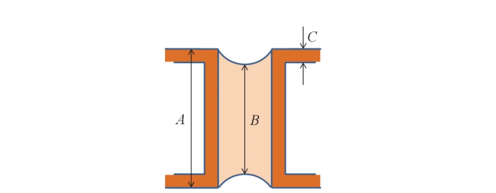
Figure 2 Schematic diagram showing how to evaluate the through hole filling performance of electroplating
1.4.2 Characterization of Via-Filling Performance
A benchtop scanning electron microscope (SEM, TM4000Plus, Japan) was used to examine whether the copper deposit on the test coupons was smooth, dense, flat, and uniform, and to check for copper nodule protrusions.
A thermal cycling shock test was used to evaluate the resistance of the plated deposit under continuous alternating temperature extremes. The maximum temperature was 125 °C and the minimum temperature was −55 °C. The coupons were held for 15 min at each high and low temperature. After 100 thermal shock cycles, the coupons were cross-sectioned; after grinding, polishing, and micro-etching, a VHX-950F 3D digital microscope (200×) was used to observe whether defects such as via cracking, voids, copper layer discontinuities, or board blowout occurred.
A solder dip thermal shock test was used to evaluate the reliability of the plated deposit. The main steps were as follows: after via filling, the coupons were baked in a constant-temperature drying oven at 150 °C for 6 h and then cooled to room temperature; the coupons were then subjected to six consecutive thermal shocks in a 288 °C lead-free solder pot, 10 s per shock. The coupons were then cross-sectioned; after grinding, polishing, and micro-etching, a 3D digital microscope (200×) was used to observe whether defects such as via cracking, voids, copper layer discontinuities, or delamination occurred.
2 Results and Discussion
2.1 Effect of Cl⁻ on Via-Filling Performance
In the base acidic copper plating solution, 8 mg/L SPS, 250 mg/L PEG-10000, 13 mg/L 2-PDS, and different mass concentrations of Cl⁻ were added to investigate the effect of Cl⁻ concentration on via-filling performance; the results are shown in Figs. 3 and 4.
As the mass concentration of Cl⁻ increased from 40 mg/L to 70 mg/L, the filling efficiency increased. Chloride ions form a complex with 2-PDS and PEG; this complex can selectively adsorb on the cathode surface, reducing the contact between copper ions and the cathode surface, thereby suppressing deposition on the board surface and at the via entrance [13–14].
In addition, the complex formed by chloride ions, SPS, and cuprous ions can reduce impedance and accelerate deposition inside the via, thereby enabling good via-filling performance.
When the Cl⁻ concentration exceeded 70 mg/L, the filling efficiency began to decrease. This may be because excess Cl⁻ in the bath reacts with Cu⁺ to form insoluble CuCl, which further forms soluble CuCl₂⁻; this species no longer adsorbs on the copper surface to effectively inhibit copper deposition, exhibiting a depolarization effect [13].
Therefore, within the tested concentration range, the filling efficiency showed a trend of first increasing and then decreasing; the dimple value decreased first and then increased, while the surface copper thickness changed little.
Based on the overall experimental results, a Cl⁻ mass concentration of 50–70 mg/L was selected as more appropriate.
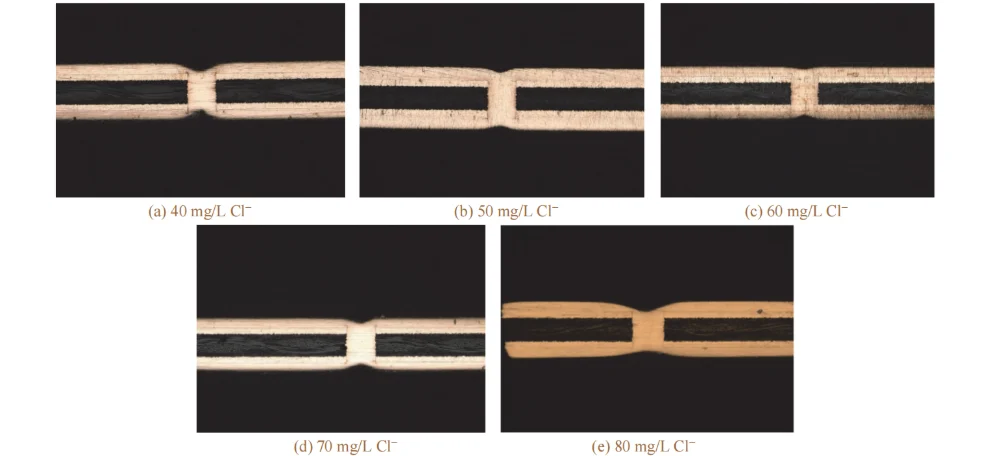
Figure 3 Cross-sectional morphologies of through holes filled by electroplating at different mass concentrations of Cl−
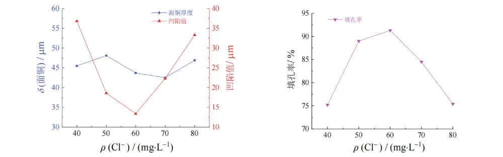
Figure 4 Effect of mass concentration of Cl− on thickness of surface copper coating, dimple, and filling efficiency of through hole
2.2 Effect of SPS on Via-Filling Performance
In the base acidic copper plating solution, 60 mg/L Cl⁻, 250 mg/L PEG-10000, 13 mg/L 2-PDS, and different mass concentrations of SPS were added to investigate the effect of SPS concentration on via-filling performance; the results are shown in Figs. 5 and 6.
As the mass concentration of SPS increased from 2 mg/L to 8 mg/L, the filling efficiency increased, and no voids were observed inside the via. This may be because SPS has a low molecular weight and, compared with the higher-current-density regions at the via entrance and the board surface, SPS tends to adsorb more readily in the low-current-density region at the via center.
During electroplating, the disulfide bond in SPS cleaves, and the generated 3-mercapto-1-propanesulfonate (MPS), in the presence of chloride ions, combines with cuprous ions (Cu⁺) to form a Cu–S–(CH₂)₃SO₃⁻ complex [15]. This complex can reduce the cathodic polarization resistance, decrease the resistance to deposition, and promote deposition inside the via.
When the SPS concentration exceeded 8 mg/L, the filling efficiency began to decrease; at 14 mg/L, the filling efficiency dropped to 60.1%. This may be because an excessively high SPS concentration weakens the suppression effects of PEG-10000 and 2-PDS on copper deposition at the board surface and via entrance, leading to more copper ion deposition on the board surface. As a result, the filling efficiency decreases, the dimple value increases, and the copper thickness increases.
Based on the overall experimental results, an SPS mass concentration of 8–11 mg/L was selected.
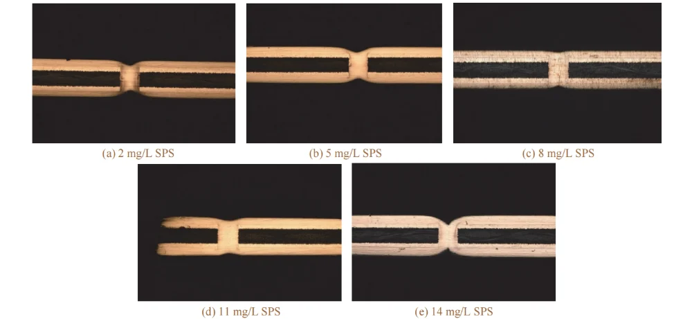
Figure 5 Cross-sectional morphologies of through holes filled by electroplating at different mass concentrations of SPS
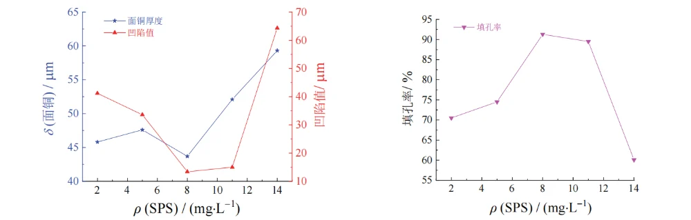
Figure 6 Effect of mass concentration of SPS on thickness of surface copper coating, dimple, and filling efficiency of through hole
2.3 Effect of PEG-10000 on Via-Filling Performance
In the base acidic copper plating solution, 60 mg/L Cl⁻, 8 mg/L SPS, 13 mg/L 2-PDS, and different mass concentrations of PEG-10000 were added to investigate the effect of PEG-10000 concentration on via-filling performance; the results are shown in Figs. 7 and 8.
When the mass concentration of PEG-10000 increased from 100 mg/L to 250 mg/L, the filling efficiency increased from 67.0% to 91.3%. This may be because this polyol-type substance can reduce the surface tension at the cathode surface, allowing the plating solution to enter the holes more easily, which is beneficial to mass transfer. In addition, CuCl formed by the combination of chloride ions and cuprous ions reacts with the added PEG-10000 to generate a complex ClCuPEG composite. This composite adsorbs on the cathode surface, enhances cathodic polarization, thereby suppressing copper deposition on the surface and increasing the filling efficiency.
When the PEG-10000 concentration was further increased to 300 mg/L, the copper thickness increased and the filling efficiency decreased. This may be because the ClCuPEG composite dissociates, and PEG becomes an intermediate in copper deposition, which affects the filling performance [16].
Therefore, a PEG-10000 mass concentration of 200–300 mg/L is more appropriate.
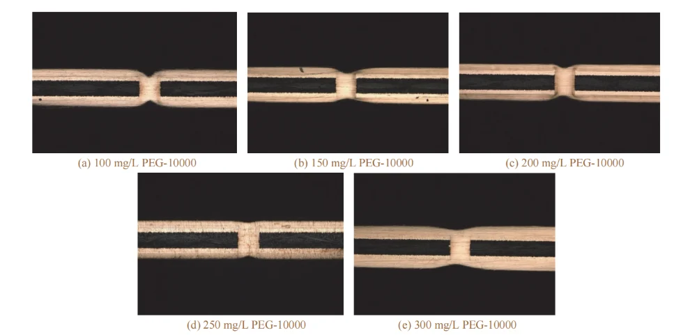
Figure 7 Cross-sectional morphologies of through holes filled by electroplating at different mass concentrations of PEG-10000
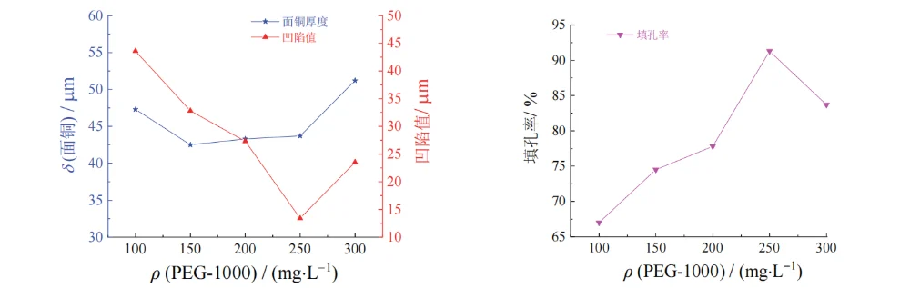
Figure 8 Effect of mass concentration of PEG-10000 on thickness of surface copper coating, dimple, and filling efficiency of through hole
2.4 Effect of 2-PDS on Via-Filling Performance
In the base acidic copper plating solution, 60 mg/L Cl⁻, 8 mg/L SPS, 250 mg/L PEG-10000, and different mass concentrations of 2-PDS were added to investigate the effect of 2-PDS concentration on via-filling performance; the results are shown in Figs. 9 and 10.
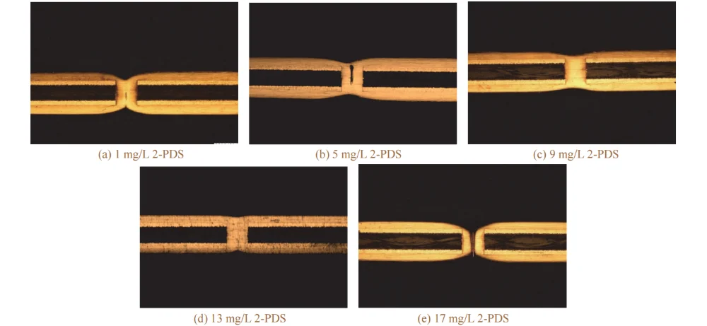
Figure 9 Cross-sectional morphologies of through holes filled by electroplating at different mass concentrations of 2-PDS
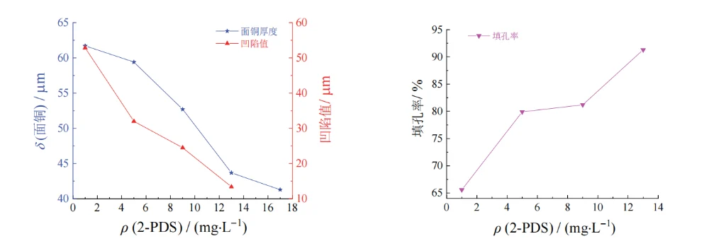
Figure 10 Effect of mass concentration of 2-PDS on thickness of surface copper coating, dimple, and filling efficiency of through hole
When the mass concentration of 2-PDS was 1–5 mg/L, the via-filling performance was poor, and voids appeared inside the holes. This is because, at such a low 2-PDS concentration, the synergistic effect of the accelerator SPS and Cl⁻ at the via entrance dominates, causing the deposition rate inside the via to be lower than that at the via entrance.
When the mass concentration of 2-PDS exceeded 5 mg/L, the filling performance gradually improved. This is because 2-PDS, which is enriched at the via entrance in the high-current-density region, forms an adsorption layer on the cathode surface, increasing the reaction resistance in the high-current-density region. This enhances suppression at the cathode surface and the via entrance, making the deposition rate at the via center higher than that at the via entrance.
However, when the mass concentration of 2-PDS exceeded 13 mg/L, the via-filling performance began to deteriorate, and the copper thickness became thinner. This may be because an excessively high 2-PDS concentration not only affects the selective suppression in the high-current-density region, but also hinders SPS from entering the via, thereby reducing current efficiency. As a result, via filling fails and the surface copper thickness decreases. Therefore, the appropriate mass concentration of 2-PDS is 9–13 mg/L.
2.5 Verification Experiments
Based on the above results, the optimized additive combination was: Cl⁻ 60 mg/L, SPS 8 mg/L, PEG-10000 250 mg/L, and 2-PDS 13 mg/L.
This additive system was introduced into the base electrolyte, and three parallel tests were carried out; the results are shown in Table 1.
Under the synergistic action of this additive combination, excellent through-hole copper via filling was achieved, with the average filling efficiency and dimple value being 91.7% and 13.6 μm, respectively, meeting industrial production requirements.
Table 1 Results of parallel experiments at optimized concentrations of additives
| Test No. | Dimple Value (μm) | Filling Rate (%) | Through-Hole Cross-Section |
| 1 | 13.9 | 91.5 | 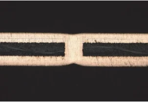
|
| 2 | 15 | 90.7 | 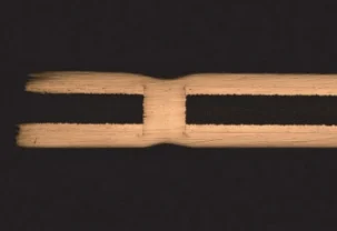
|
| 3 | 12 | 92.9 | 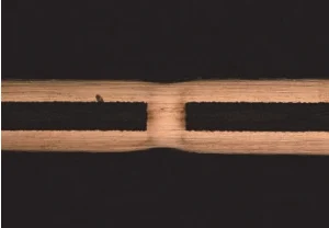
|
| Average | 13.6 | 91.7 | — |
2.6 Properties of the Copper Deposit
As can be seen from Fig. 11, the copper deposit surface is uniform, dense, and level, with no obvious copper nodules.
After the via-filled coupons were subjected to thermal cycling shock and solder dip thermal shock tests, no defects such as via cracking, voids, copper layer discontinuities, or delamination were observed in the deposit (see Fig. 12).
This indicates that the copper deposit exhibits good reliability and meets the requirements for industrial PCB production.
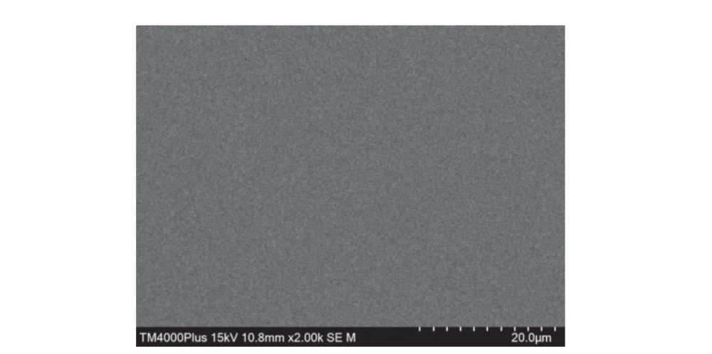
Figure 11 Surface morphology of copper coating
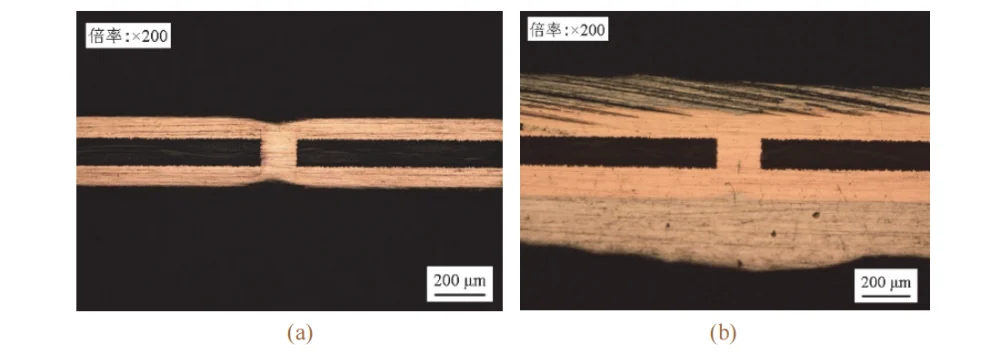
Figure 12 Metallographic images of copper-electroplated through hole after thermal shock by temperature cycling test (a) and tin immersion test (b), respectively
3 Conclusions
The effects of four additives—Cl⁻, SPS, PEG-10000, and 2-PDS—on through-hole copper electroplating via-filling performance were investigated by single-factor experiments.
The results show that in a base electrolyte composed of 75 g/L CuSO₄·5H₂O and 230 g/L concentrated H₂SO₄, the best filling performance was obtained when adding 50–70 mg/L Cl⁻, 8–11 mg/L SPS, 200–300 mg/L PEG-10000, and 9–13 mg/L 2-PDS, achieving an average filling efficiency of 91.7%, a dimple value of 13.6 μm, and a surface copper thickness of approximately 43 μm.
The copper layer surface was uniform, dense, and level, with no obvious copper nodules.
After thermal cycling and thermal stress shock tests, no defects such as board blowout, voids, via cracking, or copper layer fracture were observed, meeting the reliability requirements for industrial PCB production.
However, a limitation is that the surface copper thickness is relatively high, which is still not suitable for fine-line fabrication and requires further optimization.
References
[1] Xiao, Ning. Study on Via-Filling Performance and Mechanism of EPE-Series Copper Plating Suppressors (in Chinese) [D]. Harbin: Harbin Institute of Technology, 2013.
[2] Yan, J. J.; Chang, L. C.; Lu, C. W.; et al. Effects of organic acids on through-hole filling by copper electroplating [J]. Electrochimica Acta, 2013, 109: 1–12.
[3] Liu, Jia; Chen, Jida; Deng, Hongxi; et al. Study and optimization of through-hole copper electroplating via-filling process (in Chinese) [J]. Printed Circuit Information, 2015(3): 106–111.
[4] Lin, G. Y.; Yan, J. J.; Yen, M. Y.; et al. Characterization of through-hole filling by copper electroplating using a tetrazolium salt inhibitor [J]. Journal of the Electrochemical Society, 2013, 160(12): D3028–D3034.
[5] Kim, J. J.; Kim, S. K.; Kim, Y. S. Catalytic behavior of 3-mercapto-1-propane sulfonic acid on Cu electrodeposition and its effect on Cu film properties for CMOS device metallization [J]. Journal of Electroanalytical Chemistry, 2003, 542(1): 61–66.
[6] Dow, W. P.; Li, C. C.; Lin, M. W.; et al. Copper fill of microvia using a thiol-modified Cu seed layer and various levelers [J]. Journal of the Electrochemical Society, 2009, 156(8): D314–D320.
[7] Chen, Zhiming. Synthesis and application of a new acidic copper plating brightener SH-110 (in Chinese) [J]. Materials Protection, 1980, 13(3): 9–12.
[8] Deng, S. D.; Li, X. H.; Fu, H. Nitrotetrazolium blue chloride as a novel corrosion inhibitor of steel in sulfuric acid solution [J]. Corrosion Science, 2010, 52(11): 3840–3846.
[9] Yan, J. J.; Chang, L. C.; Lu, C. W.; et al. Effects of organic acids on through-hole filling by copper electroplating [J]. Electrochimica Acta, 2013, 109(11): 1–12.
[10] Dow, W. P.; Chen, H. H. A novel copper electroplating formula for laser-drilled microvia and through-hole filling [J]. Circuit World, 2004, 30(3): 33–36.
[11] Chen, C. H.; Lu, C. W.; Huang, S. M.; et al. Effects of supporting electrolytes on copper electroplating for filling through-hole [J]. Electrochimica Acta, 2011, 56(17): 5954–5960.
[12] Lin, Jindu; Wu, Meizhu. Copper electroplating technology and development for PCB (in Chinese) [J]. Printed Circuit Information, 2009(12): 27–32.
[13] Tang, Mingxing; Zhang, Shengtao; Chen, Shijin; et al. Effects of additives on copper filling performance in PCB micro blind vias (in Chinese) [J]. Electroplating & Finishing, 2017, 36(13): 667–673.
[14] Liao, Chaohui; Zhang, Shengtao; Chen, Shijin; et al. Comparative study of tricyclazole and organic solder mask films on inhibiting copper corrosion in sulfuric acid and sodium chloride solutions (in Chinese) [J]. Electroplating & Finishing, 2018, 37(17): 755–761.
[15] Wang, Chong. Molecular Simulation of Additives for Through-Hole Copper Electroplating in PCB and Study on Their Mechanisms (in Chinese) [D]. Harbin: Harbin Institute of Technology.
[16] Gabrielli, C.; Mocotéguy, P.; Perrot, H.; et al. A model for copper deposition in the damascene process [J]. Electrochimica Acta, 2007, 51(8): 1462–1472.
 en
en

.jpg)
 WhatsApp