Introduction: The Demands of Modern Power Electronics
In today's world of high-power systems—electric vehicles, renewable energy converters, industrial drives, and aerospace propulsion—the efficiency and reliability of power modules depend on the performance of their printed circuit boards. Traditional substrates like FR-4 or metal-core PCBs struggle under the extreme heat, voltage, and current densities required by these applications.
")
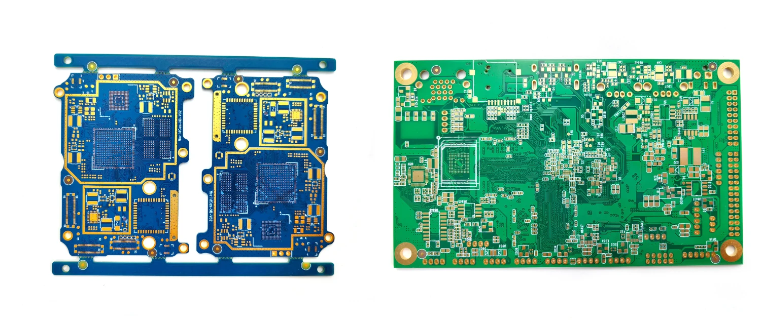
Enter the Ceramic Printed Circuit Board (PCB) — a material engineered to handle high current and temperature environments where others fail. Built from Alumina (Al₂O₃), Aluminum Nitride (AlN), or Silicon Carbide (SiC), ceramic PCBs deliver thermal conductivity up to 220 W/m·K and operate reliably between –55°C and 800°C.
For power module engineers, ceramic PCBs offer unmatched thermal management, electrical insulation, and mechanical stability, making them the preferred choice for next-generation high-efficiency systems.
Why Ceramic PCBs Are Essential for Power Modules
Power modules combine semiconductor devices such as IGBTs, MOSFETs, and diodes with driver circuits and cooling structures. These modules are designed to handle hundreds of volts and amperes—conditions that generate significant thermal stress.
Ceramic substrates excel in these environments due to six key advantages:
Unrivaled Thermal Management: Efficient heat conduction prevents junction overheating.
Extreme-Temperature Stability: Stable performance up to 800°C.
Superior High-Frequency Performance: Ideal for fast-switching devices.
Ultra-High Density & Miniaturization: Supports compact, multi-layer layouts.
Zero Degradation in Harsh Conditions: Resistant to oxidation and corrosion.
High Voltage/Current Reliability: Strong dielectric insulation under load.
Together, these properties make ceramic PCBs a critical enabler for high-performance, long-lasting power electronics.
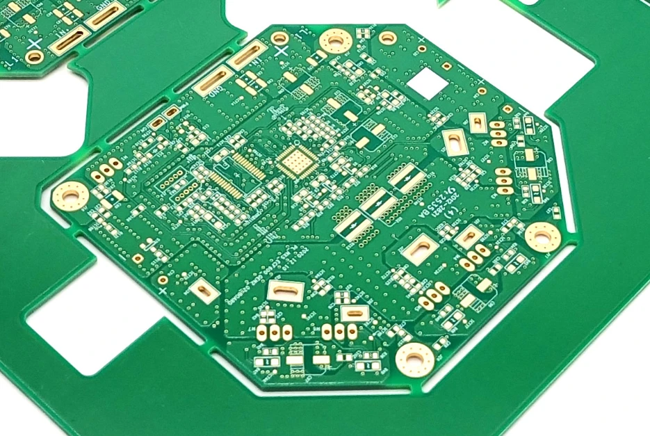
Heavy-Copper Ceramic PCB: Handling High Current Loads
Power modules often require thick copper conductors—known as heavy-copper PCBs—to carry large current loads efficiently.
In a heavy-copper ceramic PCB, copper layers range from 100 µm to over 400 µm and are bonded directly onto the ceramic substrate using Direct Bonded Copper (DBC) or Direct Plated Copper (DPC) technology.
Advantages of Heavy-Copper Ceramic PCBs:
High Current Capacity: Supports large current flow without thermal damage.
Low Thermal Resistance: Rapid heat transfer reduces temperature gradients.
Improved Mechanical Strength: Thick copper layers enhance board durability.
Reliable Metallization: Excellent adhesion between copper and ceramic prevents delamination.
This configuration is ideal for high-power applications such as EV inverters, industrial drives, and renewable energy systems.
Key Manufacturing Technologies for Power Ceramic PCBs
1. Direct Bonded Copper (DBC)
A proven technology where copper foil is bonded directly to ceramic under high temperature. DBC creates a strong metallurgical bond, ensuring superior heat conduction and mechanical integrity.
Thermal Conductivity: Up to 200 W/m·K (AlN-based)
Applications: IGBT modules, rectifiers, motor drivers
2. Direct Plated Copper (DPC)
DPC uses sputtering and electroplating to create thinner, high-precision copper traces on ceramic substrates. It’s ideal for miniaturized, high-density power circuits.
Benefits: Fine-line circuits, high-frequency performance
Applications: DC/DC converters, power amplifiers
3. Thick-Film Metallization
Conductive pastes containing silver or copper are printed and fired onto ceramic surfaces to form resistors, conductors, and dielectric layers.
Advantages: Cost-effective and customizable
Applications: Power sensors, control modules, and hybrid circuits
Each process requires tight control of temperature, metallization, and adhesion parameters to achieve high-reliability performance in power modules.
Thermal and Electrical Advantages of Ceramic PCBs
Property | Ceramic PCB | FR-4 / Metal Core PCB |
Thermal Conductivity | 18–220 W/m·K | 0.25–5 W/m·K |
Operating Temperature | –55°C to +800°C | –40°C to +130°C |
Dielectric Strength | >15 kV/mm | <4 kV/mm |
Coefficient of Thermal Expansion (CTE) | 4–8 ppm/°C | 16–18 ppm/°C |
Corrosion Resistance | Excellent | Limited |
Thermal Cycling Endurance | High | Low |
Ceramic PCBs provide both thermal efficiency and electrical insulation in a single substrate, eliminating the need for additional insulation or thermal interface materials. This significantly improves system reliability and simplifies thermal design.
Power Module Applications for Ceramic PCBs
1. Electric Vehicle Inverters and Chargers
EVs rely on high-efficiency power conversion. Ceramic PCBs ensure reliable operation under rapid load changes and wide temperature ranges. AlN-based boards are especially suited for compact, high-current inverters and on-board chargers.
2. Renewable Energy Converters
Solar and wind inverters demand high durability under fluctuating power conditions. Ceramic PCBs’ superior heat resistance prevents fatigue and delamination, ensuring stable power delivery.
3. Industrial Drives and Automation
Ceramic substrates withstand vibration and continuous thermal cycling in servo drives and robotic controllers. Their dimensional stability ensures consistent alignment in high-speed motor systems.
4. Aerospace and Defense Power Systems
High-temperature and radiation-resistant SiC ceramic PCBs are used in avionics and propulsion systems, maintaining performance where traditional substrates fail.
5. Power Amplifiers and RF Devices
With low dielectric loss and high frequency stability, ceramic PCBs enable clean, distortion-free signal transmission in high-speed communication and radar systems.
Design Considerations for High-Current Ceramic PCBs
Copper Thickness: Choose 200–400 µm copper for high-current paths.
Thermal Simulation: Optimize copper layout to minimize hotspots.
Substrate Material:
Al₂O₃: Cost-effective for moderate power.
AlN: For high-current, high-heat applications.
SiC: For ultra-high-temperature or aerospace environments.
Surface Finish: ENIG or silver plating ensures excellent solderability and oxidation resistance.
Insulation Distance: Maintain adequate creepage for high-voltage safety.
By integrating these considerations, engineers can create compact, thermally efficient, and durable power modules with maximum energy efficiency.
Why Benlida Circuit Leads in Ceramic Power PCBs
Benlida Circuit specializes in manufacturing high-performance ceramic PCBs for global power electronics markets. With advanced DBC, DPC, and thick-film capabilities, Benlida produces heavy-copper, high-current boards designed to meet demanding automotive, industrial, and energy system standards.
Every board undergoes rigorous testing — including electrical, thermal, and reliability validation — to ensure superior performance and long service life.
To explore advanced ceramic PCB solutions for power modules, visit Benlida's Ceramic PCB page for detailed product and process information.
Conclusion: Powering the Future with Ceramic PCB Technology
From electric mobility to renewable energy, the shift toward high-efficiency power systems demands materials that can withstand heat, voltage, and mechanical stress. Ceramic PCBs provide the foundation for this transformation — combining heavy-copper capability, superior thermal performance, and long-term reliability.
By adopting ceramic technology, engineers can design more compact, powerful, and efficient modules, pushing the limits of modern power electronics.
Benlida Circuit continues to lead this evolution, delivering cutting-edge ceramic PCB solutions built for the future of high-power and high-temperature applications.
 en
en

.webp)
 WhatsApp