Home > Blog > Industry News > SMT PCB Board Assembly: Industry Best Practices for High-Density Component Placement
SMT PCB Board Assembly: Industry Best Practices for High-Density Component Placement
Share
Dec 01
Source:
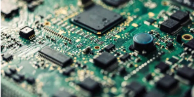
You face many problems with high-density electronic designs. SMT PCB Board Assembly helps fix issues like too many parts, signal problems, and tight spaces for routing. Benlida uses years of skill and new technology to help you get good results. You must watch stack-ups, micro-vias, and pick smart components. Here are some common problems you may see:
Layer order changes routing and signal strength.
Micro-vias help routing but need good planning.
Too many parts close together can cause problems.
Choosing the best materials makes things work better.
Key Takeaways
Plan your layout with care. Put related components close together. This helps routing and makes performance better.
Start using optical inspection systems early. These systems find defects before they get worse. This helps keep quality high.
Pick the right materials and components. This makes solder joints stronger. It also makes the board more reliable.
Follow IPC guidelines for design and assembly. These rules help lower errors and make more good boards.
Best Practices for High-Density SMT Assembly
Direct Approach to SMT PCB Board Assembly
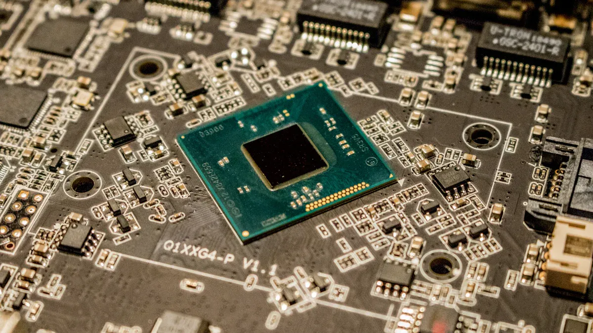
You need a good plan for high-density designs. First, put related components close together. This helps you use fewer vias. It also makes the board work better. Place SMT components facing the same way. This makes it easier to put them on the board. It also lowers mistakes. Automated pick-and-place machines help you work faster. These machines use vacuum nozzles and cameras. They can place thousands of parts every hour.
Tip: Fast placement machines can put up to 85,000 parts each hour. Smart inspection systems, like CYBEROPTICS, can lower misalignments by over 70% in tricky modules.
You should use automated assembly lines too. These lines help you keep things precise. They also lower human mistakes. Add optical inspection systems early in the process. These systems find problems before they get worse. Keep your stencil printer clean for good solder paste. Use the same component sizes and packages. This helps you avoid changing machine settings often. Work with suppliers to get good parts on time.
Here are some best practices you can use:
Put related components together to help routing and performance.
Face components in one direction for easy placement.
Use automated pick-and-place machines for better accuracy.
Add optical inspection systems to find defects early.
Keep solder paste printing steady for good results.
Use the same component sizes to save setup time.
Work with suppliers for good parts when you need them.
These steps help you place parts more accurately. Good alignment during reflow soldering makes strong solder joints. This lowers defects and raises yield rates. Even a tiny mistake, like 0.05 mm, can make soldering problems go up by 30%. You need to watch every detail in SMT PCB Board Assembly.
Key Factors for Reliability and Manufacturability
You want your boards to last and work well. Focus on these things to make your boards strong and easy to build:
Factor
Description
Material selection
Pick materials that make strong solder joints and steady boards.
PCB design
Use smart design to keep signals steady and stop board breaks.
Manufacturing process
Keep drilling and etching the same to avoid problems like board layers coming apart or broken paths.
Assembly process
Make sure your assembly makes strong solder joints. Test early to find problems.
Environment and Conditions
Test boards to handle heat, water, and other tough things.
Watch out for common design mistakes. Solder problems, like bridges and tombstoning, cause most SMT issues. Footprint mistakes can lower your first-pass yield by up to 25% in high-density boards. Careful planning and testing help you stop these problems.
Follow these steps for better solder paste use:
Pick the right stencil thickness for your parts. Use 0.1 mm for tiny parts.
Match hole sizes to pad sizes. Make holes 10-20% smaller for better paste release.
Keep at least 0.1 mm of solder mask around pads. This stops solder bridges.
New trends are changing SMT PCB Board Assembly. Automation helps you work faster and make fewer mistakes. Smaller parts let you fit more on the board. Better materials make boards work better. Quality control matters more as boards get harder to build. Sustainability and optical inspection systems are also more important.
Note: You can get better results by using automated inspection and focusing on quality control. These steps help you find problems early and keep your boards working well.
When you use these best practices, your SMT PCB Board Assembly gets stronger and more reliable. You get more good boards and fewer mistakes. Your boards work better and last longer.
High-Density Placement: Importance & Challenges
Why High-Density Matters
High-density placement is used in many new electronics. Phones, servers, and AI hardware need to be fast and small. More parts must fit on each board to meet these needs. High-density layouts save space and make things work better.
Here are some facts about high-density:
High-density data centers use less space and work better.
These centers have racks that use 40 kW to 200 kW of power.
Some CPUs use 400 W, and AI GPUs can use 1000 W.
High-density placement keeps devices small and strong. SMT PCB Board Assembly lets you put more parts on a board. This helps you make faster and smarter products for today.
Tip: High-density designs help save money and energy. You get more from every inch of your board.
Common Challenges in Dense PCB Layouts
Dense PCB layouts have many hard problems. Each problem can hurt how well your board works. You need to plan well to stop these problems.
Challenge Type
Description
Material selection
Pick materials with steady dielectric constants and smooth copper for good signals.
Component placement
Put parts with the same signals together. Keep radiators away from other parts.
Spacing and clearances
Keep the same space between traces. Follow safety rules for spacing.
Routing
Put different signals on different layers. Keep traces short for better signals.
Stackup
Use a balanced stackup to stop the board from bending.
Grounding
Use different grounds for each signal. Do not split ground planes.
Filtering
Add filters to boards with fast switching to lower EMI.
Shielding
Use shields for parts that give off lots of radiation.
You need to check every step in your design. Small errors can cause big issues like signal loss or too much heat. Good planning and smart layout choices help you make strong and safe boards.
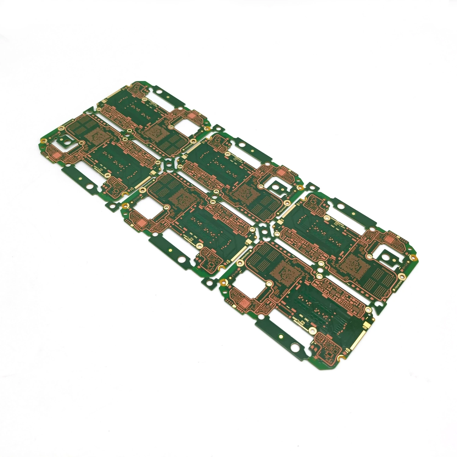
PCB Stack-Up & Layer Design
Signal Integrity Strategies
It is important to keep signals strong in high-density PCB designs. Signal integrity means signals stay clear and do not get noisy. You can use smart ways to protect signals. Here is a table with some top methods:
Strategy
Description
Material Selection
Pick materials with low dielectric constant and dissipation factor. This helps stop signal distortion and energy loss.
Layer Arrangement
Put signal layers between ground planes. This shields signals from electromagnetic interference and gives low-impedance return paths.
Trace Routing
Use controlled impedance routing. This stops reflections and keeps signals strong.
Signal Integrity Management
Lower crosstalk and use good termination. This keeps signals clean on all layers.
Tip: You can make signals better by keeping traces short. Use ground planes as shields. This helps your board work faster and more reliably.
Layer Arrangement for Manufacturability
You need to plan your layer arrangement so your board is easy to build and strong. Good stacking helps you avoid problems when making the board. Buried microvias are important. These tiny connections do not reach the surface. Design them with a low aspect ratio and make them span only one layer. This makes building easier and connections stronger.
You can follow these steps to help manufacturability:
Stack layers well to use fewer vias. This makes building easier.
Put ground and power planes in smart spots. This helps with heat and keeps your board stable.
Keep your design small. This lowers the risk of delamination from different materials.
Use microvias instead of common vias to boost routing density.
Put ground and power layers at the top of the stack-up. This can remove the need for extra vias.
Use microvias to free up space on other layers. This makes your design more compact.
Note: Careful layer arrangement helps you build boards that last longer and work better. You get fewer defects and stronger connections.
Via Selection for Dense Routing
Micro-Via Usage
You use microvias when you need many connections in a small area. Microvias help signals move between layers without using much space. You can put microvias inside the pads of surface-mount parts. This saves space and lets you make smaller, faster boards.
Microvias also help signals stay clean. Their small size means less unwanted effects. You get better signals, which is important for fast circuits. Laser-drilled microvias have fewer problems than bigger, drilled vias. You can trust them for better results in HDI designs.
But, you must be careful about reliability. Microvias can break during plating or when the board heats and cools. You need to plan well and work with good manufacturers to stop these problems.
Here is a table that shows the main good and bad points of microvias:
Advantage/Limitations
Description
Space Savings
Microvias let you fit more connections and go inside SMT pads, saving space.
Signal Integrity
Microvias lower unwanted effects, making signals better.
Reliability Concerns
Microvias might break during plating or heating, so reliability can drop.
Reduced Signal Radiation
Smaller microvias lower signal radiation and reflection.
Lower Manufacturing Defects
Laser-drilled microvias have fewer problems than bigger, drilled vias.
Tip: You can make your board work better by using microvias in important signal paths.
Choosing the Right Via Type
You need to choose the best via type for your board. Conductive fills are good when you want strong electrical paths and better heat flow. You should use them in fast or power boards. Non-conductive fills help keep pads steady during assembly. They are best when you want to stop solder wicking and save money.
Here is a table that compares conductive and non-conductive fills:
Aspect
Conductive Fills
Non-Conductive Fills
Electrical Performance
Makes connections stronger, good for fast boards
Better for keeping things apart, does not help signals
Thermal Management
Helps heat move away, good for power boards
Not as good at moving heat, less helpful for heat
Structural Integrity
Gives support, but not as good at stopping solder wicking
Best for keeping pads steady during assembly
Application Suitability
Used in HDI and RF boards
Used in normal multilayer boards to save money
You can make your board stronger and work better by picking the right via type. Always check what your board needs before you decide.
Component Placement Rules
Grid System for Placement
You can use a grid system to put parts on your PCB. This way, everything stays neat and tidy. Each part goes on a grid spot. You do not place parts randomly. The grid system makes routing simple. You can plan trace paths without crossing other parts. This lowers mistakes during assembly.
Here are some good things about using a grid system:
Parts stay lined up for machines.
Inspection is quicker and more exact.
Design changes and repairs are easier.
Soldering mistakes happen less often.
Tip: Pick a grid size that fits your smallest part. For example, use a 0.5 mm grid for fine-pitch ICs. This keeps spacing even and stops crowding.
A grid system helps you follow rules in the industry. You meet IPC guidelines for spacing and placement. Your board is easier to build and test.
Grouping & Heat Management
You should put parts with the same job together. This makes your PCB easier to read and fix. Keep analog parts away from digital parts. Also, separate high-power parts from sensitive circuits. Grouping helps you control noise and signal problems.
Heat management matters in high-density designs. Put hot parts, like power ICs and regulators, away from heat-sensitive parts. Use thermal vias to move heat to other layers. Add copper pours under hot parts to spread heat.
Heat Management Method
How It Helps You
Thermal Vias
Moves heat away from hot spots
Copper Pours
Spreads heat across the PCB
Component Spacing
Prevents overheating
Note: Always check the datasheet for each part. You find the best spot and cooling method for your design.
You make your board work better and last longer by following these rules. Your board stays cool and works well. You also make assembly and testing simpler.
SMT PCB Board Assembly Process
Solder Paste Printing
You begin with solder paste printing. This step puts small bits of solder paste on each pad. Pads are where you will place the components. Benlida uses machines with cameras for accurate work. These machines help you avoid mistakes. They make sure every pad gets covered. New technology makes this step better. For example, 3D solder paste inspection checks the height and shape of each paste spot. Nano-coating on stencils keeps the paste even and means less cleaning. Smart stencils have sensors to watch pressure and temperature. They give you feedback right away.
Innovation
Description
3D Solder Paste Inspection
Checks solder paste deposits for accuracy and defects.
Nano-Coating Technology
Improves consistency and reduces cleaning needs.
Smart Stencils
Monitors printing conditions and extends stencil lifespan.
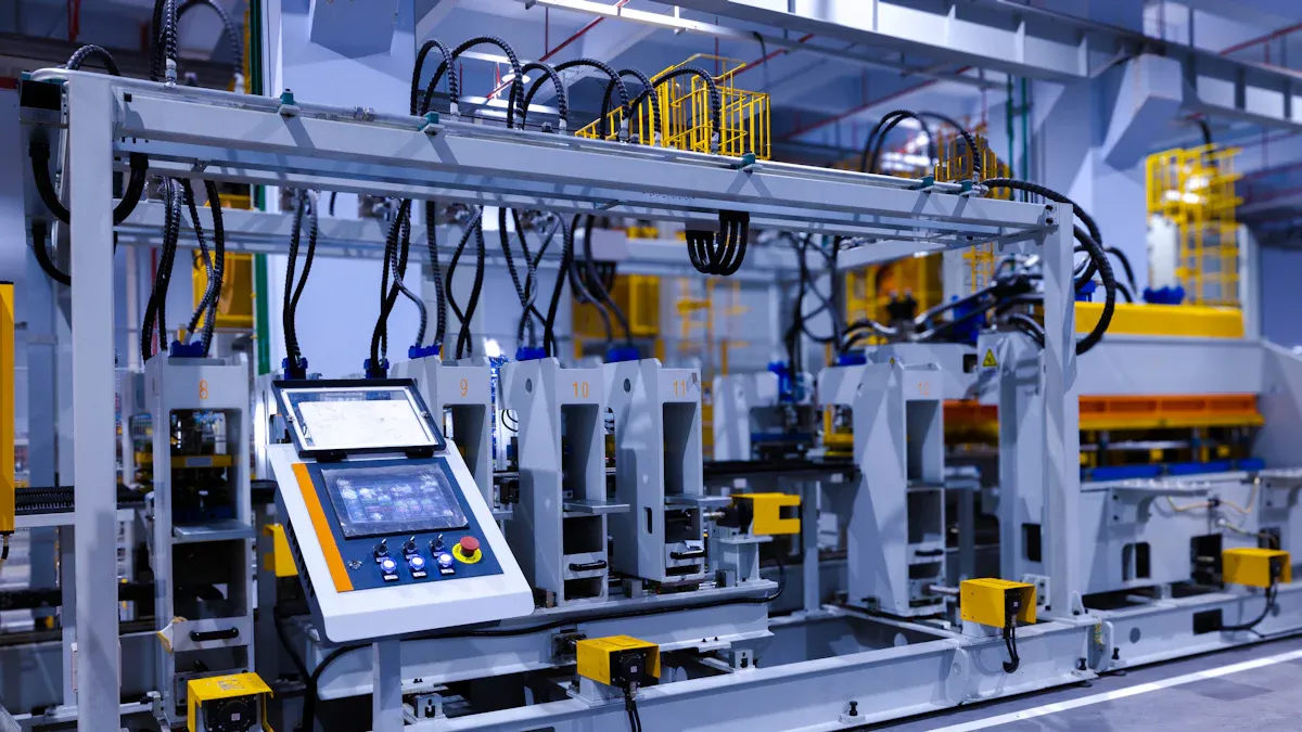
Automated Pick-and-Place
Next, you use pick-and-place machines. These machines grab each part and put it in the right spot. Benlida’s equipment uses cameras and robots for good alignment. You get better accuracy and faster work. The machines work quickly and keep mistakes low. They can handle thousands of tiny parts.
Advantage
Description
More precision
Vision systems align parts with high accuracy.
Higher production efficiency
Automation speeds up placement and keeps quality consistent.
Tip: Pick-and-place machines help you build boards fast and with accuracy.
Reflow Soldering
After placing parts, you do reflow soldering. This step melts the solder paste and connects each part to the board. You follow a careful heating plan to avoid damage. Benlida uses ovens and nitrogen to stop oxidation. Each step is important:
Step
Description
Importance
Initial Heating
Raises temperature slowly.
Prevents splattering and protects components.
Thermal Soak
Holds temperature steady for 1-2 minutes.
Avoids defects like graping and head-in-pillow.
Reflow
Melts solder and forms strong joints.
Ensures good connections without thermal damage.
Cooling
Lowers temperature to solidify joints.
Makes solder joints strong and free of defects.
Nitrogen Environment
Keeps oxygen away during reflow.
Improves solder quality and reduces defects.
Inspection & Testing
You finish with inspection and testing. Benlida checks every board in many ways. Automated Optical Inspection uses cameras to look for solder problems. X-ray systems check hidden joints and inside layers. Flying probe and functional tests make sure every connection works. These steps help you find problems early and give you reliable boards.
Inspection Method
Description
Automated Optical Inspection (AOI)
Uses cameras to inspect solder joints and placement.
X-Ray Fluoroscopic System
Checks internal solder joints and distribution.
Flying Probe Testing
Verifies electrical connections and performance.
Note: Benlida’s advanced tools and strict checks help you get strong SMT PCB Board Assembly for high-density designs.
Industry Standards & Quality Assurance
IPC Guidelines
You must follow strict rules when making high-density SMT PCB boards. IPC guidelines help keep your boards safe and reliable. These rules show you how to design, build, and check your boards. Benlida uses these rules for every step. Using the right IPC standards gives you better boards.
IPC Standard
Description
IPC-7351
Land pattern design rules. You get the right pad sizes and spacing for surface-mount parts.
IPC-A-610
Quality rules for electronic assemblies. You see what good solder joints and placement look like.
IPC-J-STD-001
Soldering process rules. You learn about materials and setup for strong solder connections.
You can use IPC-7351 footprint libraries. This helps you pick the right pad sizes and spacing. You should use IPC standards in your drawings. This keeps you and your partners working together. Train your team on IPC rules. You get better boards every time.
Tip: IPC guidelines help you stop mistakes and keep your boards working.
Documentation & Traceability
You need to keep good records when making high-density SMT PCB boards. Documentation and traceability help you track every part and step. This makes your boards safer and easier to fix. Benlida uses strong traceability systems to check every board.
You can track each part and step. This keeps your product strong and reliable.
You meet rules for making high-density SMT PCB boards.
You find problems fast. This helps you fix things and make your process better.
Benlida’s quality checks use good documentation and traceability. You get boards that meet strict rules. You can trust your boards to work well anywhere.
Note: Good records and traceability help you fix problems fast and keep your products safe.
Mistakes to Avoid & Optimization Tips
Common Pitfalls in High-Density SMT
Designing high-density SMT PCB boards is tough. Small errors can cause big trouble. You need to watch for common mistakes. Here is a table that shows some problems and ways to fix them:
Common Pitfall
Description
How to Avoid This Mistake
Insufficient component spacing
Wrong footprints can cause soldering problems.
Check the footprint with the datasheet before you finish your layout.
Poor placement of fiducial marks
Missing fiducials can make parts line up wrong during assembly.
Put at least two fiducial marks on opposite corners. Keep them away from edges and big parts.
Ignoring thermal management
Too much heat can break parts.
Use thermal vias and copper pours to spread heat across the board.
Inadequate solder mask and silkscreen
Bad design can cause solder bridges and confusion.
Make solder mask openings a bit bigger than pads. Add clear marks for part direction.
Tip: Always look over your design files before sending them to be made. You can find many problems early and save time.
Practical Design Optimization
You can make your high-density SMT PCB boards better by using smart steps. Group parts that do the same thing together. This makes routing easier. Use a grid system to place parts. This keeps everything lined up and helps with inspection.
Watch out for heat. Put hot parts away from sensitive ones. Add thermal vias under power parts. Use copper pours to spread heat. This keeps your board cool and safe.
Here are some quick tips to help you:
Pick the smallest footprints for your parts.
Keep traces short for better signals.
Add clear silkscreen marks for every part.
Put fiducial marks in open spots for good alignment.
Go over your design with your assembly partner before making it.
Note: You make your board stronger and more reliable when you use these steps. Good planning helps you avoid expensive mistakes and build strong, high-density SMT PCB boards.
You can make your SMT PCB Board Assembly better by using smart steps. Use small components to save space on the board. Try double-sided layouts to fit more parts. Automated pick-and-place machines help you work faster. These machines also lower mistakes. Short leads help signals move faster. This is important for high-frequency boards. Benlida gives you good service and strong quality checks.
Item
Best-Practice Guideline
Why It Matters
Design for Manufacturability
Use IPC standards for layout and land patterns
Fewer mistakes and better yield
Stencil & Paste Optimization
Pick the right stencil thickness and aperture changes
Good solder paste and fewer defects
Design for Test
Add test features during design
Easier testing and fixing
Remember: Good planning and smart choices help you build strong boards every time.
FAQ
What is the main benefit of high-density SMT PCB assembly?
You can put more parts on a small board. This makes devices smaller and faster. You can add more features without making the product bigger.
How do you avoid soldering defects in high-density boards?
Use the right stencil thickness for your board. Keep the solder paste printer clean all the time. Automated inspection tools help you find mistakes early. Always check your design before you start assembly.
Why do you need microvias in dense PCB layouts?
Microvias connect layers in tight spaces. You can route more signals without using much space. This keeps your board small and your signals strong.
How does Benlida ensure quality in SMT PCB assembly?
Benlida uses advanced machines and strong testing. You get Automated Optical Inspection, X-ray checks, and flying probe tests. These steps help you get reliable boards every time.
This website uses cookies to provide you with a safer and more personal experience. By accepting, you agree to the Cookie Policy and the use of cookies for advertising and analytics purposes.
 en
en


 WhatsApp