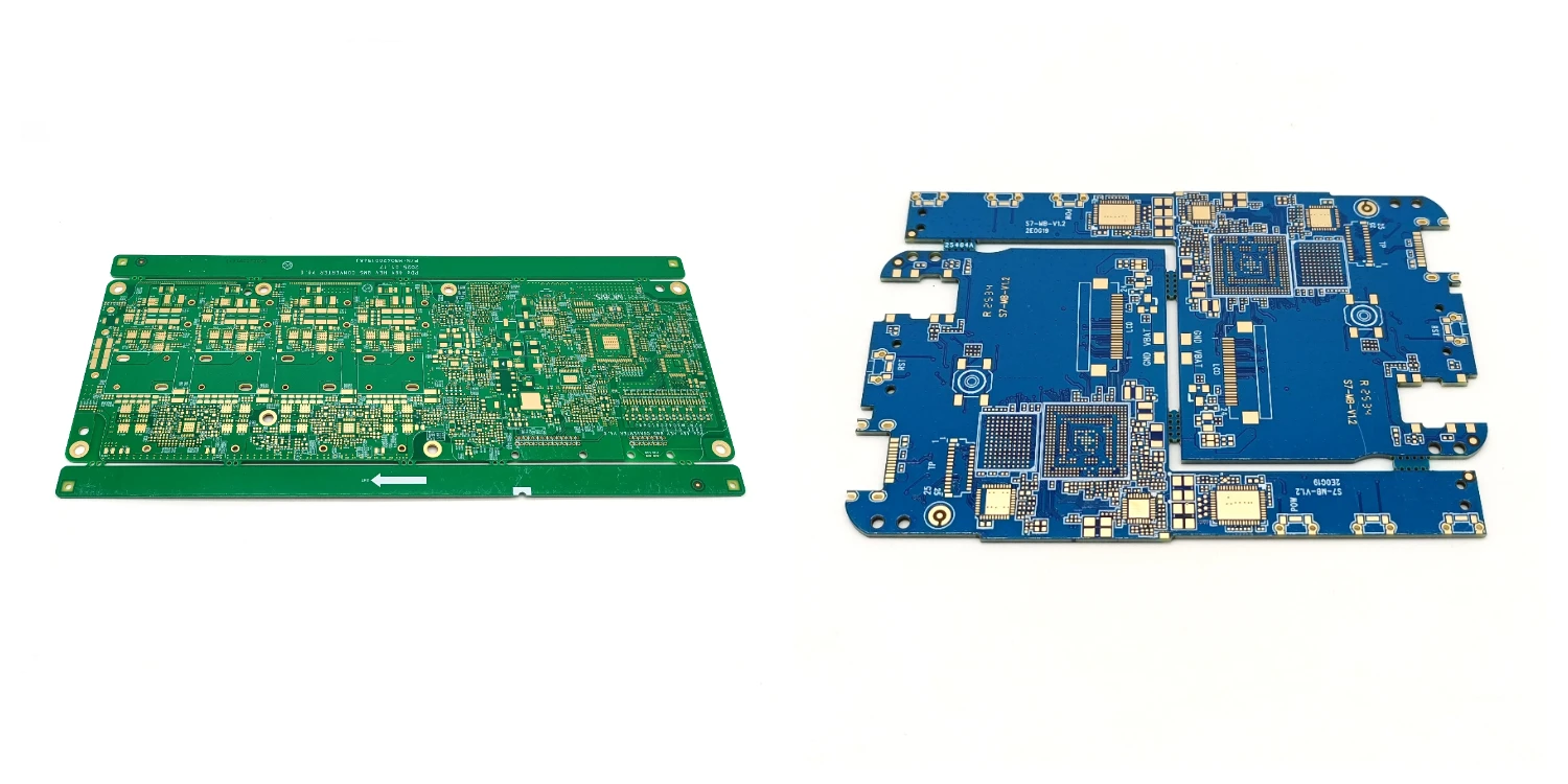
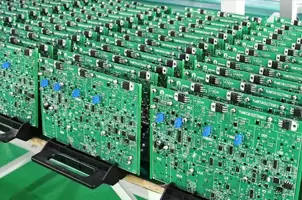
ENIG (Electroless Nickel Immersion Gold) is one of the most commonly applied surface treatment in morden PCB industry. It's advantages include: lead-free, easy to solder, oxidation-resistance, even the manufacturing cost is higher than other approaches such as OPS and HASL, but still it is more tend to be applied on high-value, high-density, high-quality, BGA package, and RoHS-compliant PCBs, such as electronics for medical, smartphone, telecommunication and military.
One of the defects around ENIG is black pad, also called as Phosphorus-Rich layer. It normally shown up as dark spots on the nickel layer under the gold. These spots are caused by nickel corrosion. Below are the formation, characteristics and negative effects of it:
I. Formation of Black Pad/Phosphorus-rich Layers
Phosphorus-rich layers are mainly formed during two steps of the electroless nickel immersion gold (ENIG) process:
1. Electroless Nickel Plating Process (Forming of Ni-P Layer):
In the ENIG process, the surface deposited on the pads is not pure nickel, but nickel-phosphorus alloy. The reducing agent in the plating bath (such as sodium hypophosphite) reduces and deposits nickel ions under catalysis, while phosphorus (P) is also co-deposited into the coating. Based on phosphorus content, it can be divided into low phosphorus (2-5%), medium phosphorus (6-9%), and high phosphorus (>10%). Medium phosphorus coatings are commonly used in ENIG.
2. Immersion Gold (leading to phosphorus enrichment):
● Immersion gold is performed after nickel plating. Immersion gold is a chemical displacement reaction: gold ions displace nickel atoms from the nickel layer surface in the plating bath, the nickel atoms dissolve into the gold solution, and gold atoms deposit on the nickel layer surface.
● This displacement reaction selectively corrodes the nickel layer; nickel atoms are selectively dissolved, while phosphorus atoms do not participate in the reaction and are not dissolved in the gold solution.
● Therefore, during the immersion gold process, nickel atoms on the nickel layer surface are continuously dissolved, leaving behind phosphorus atoms. This forms an extremely thin layer at the top of the nickel layer with a phosphorus concentration far higher than the bulk nickel layer—this is the "phosphorus-rich layer." Its phosphorus content can be as high as 20% or more (atomic percentage).
In summary: The phosphorus-rich layer is a product of the selective corrosion and dissolution of nickel during the ENIG immersion gold process, resulting in the residual and enriched phosphorus atoms at the nickel-gold interface.
II. Characteristics of the Phosphorus-Rich Layer
1. Chemical Composition: The main components are phosphorus (P) and some nickel (Ni), possibly existing as amorphous nickel-phosphorus compounds (such as Ni3P).
2. Morphology and Thickness: Very thin, typically only tens to hundreds of nanometers (nm), located at the interface between the nickel layer (Ni-P) and the gold layer (Au), appearing as a bright, thin line under electron microscope.
3. Physical Properties: High resistivity, its most critical characteristic and the main reason for its adverse effects on circuit board performance: The resistivity of the phosphorus-rich layer is much higher than that of metallic nickel and gold, making it a poor conductor of electricity.
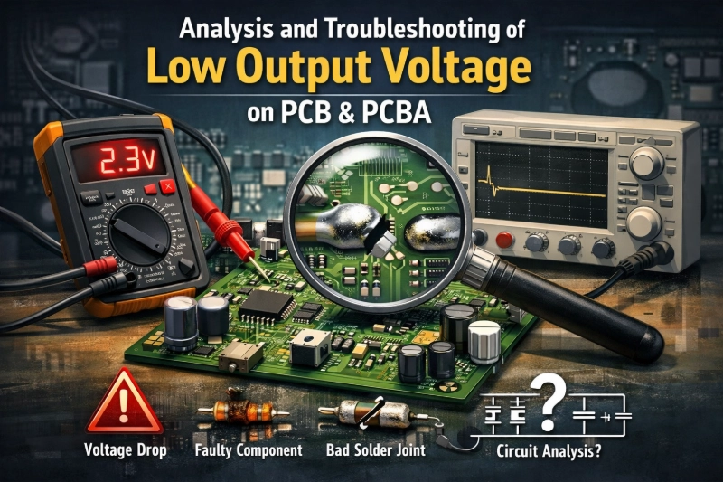
III. Adverse Effects of the Phosphorus-Rich Layer on Soldering Reliability:
1. "Black Pad" Defect: This is the most serious quality defect caused by the phosphorus-rich layer. If the immersion gold process is out of control (e.g., too long, too active gold fluid), it will lead to excessive corrosion, forming an excessively thick, continuous phosphorus-rich layer. During soldering, after the surface gold layer dissolves, the solder encounts the high-resistivity phosphorus-rich layer, but not the nickel layer.
2. Poor solderability and cold solder joints: The solder cannot form an effective metallurgical bond with the high-resistivity phosphorus-rich layer (difficult to form good Ni3Sn4 IMC), resulting in poor solder joint wetting, cold solder joints, and extremely low connection strength.
3. Weak solder joint: Even if a solder joint is formed, the interfacial bonding is very weak, and it is tend to crack from the phosphorus-rich layer, when under mechanical force or thermal shock.
Benlida is technical expert in PCB manufacturing for 14 years. With years of process optimization and technical upgrades, it is expert to avoid the "black pad" defect on ENIG. Relying on professional equipments and engineering&quality team, Benlida is also providing analysis services and solutions:
● High-resolution scanning electron microscopy and energy dispersive spectroscopy, cross-sectional analysis of the solder pads, clearly observe the presence, thickness, and continuity of the phosphorus-rich layer, therefore analyze the elements, formation cuases accurately, provide data for process analysis.
● Analysis for "Black Pad" Defect : When solder joints has issues such as non-wetting, poor soldering, or insufficient strength, our quality team analyze the reasons of the failure is caused by a "black pad" defect resulting from the phosphorus-rich layer through microstructural analysis, thus pinpointing the root cause of the process problem.
● Process Optimization: By comparing and analyzing the interface conditions under different nickel plating/immersion gold process parameters, we assist customers in optimizing the ENIG process, inhibiting excessive phosphorus-rich layer growth, and improving soldering yield and reliability from the source.
● Comprehensive Reliability Testing: We provide reliability tests such as thermal cycling and high-temperature/high-humidity testing to assess the long-term reliability of solder joints and evaluate the potential risks caused by defects.
If your project encounters problems such as black pads, poor appearance, solder pad lose, poor appearance, poor soldering, or solder joint cracking, relating to surface treatment ENIG, please contact Benlida to know more about our production processes and quality control. To support our customers, we offer competitive price and and consultation services. With professional production facility, engineering and quality engineers, Benlida is happy to manufacture good PCB for you!
 en
en


 WhatsApp