What is PoP(Package-on-Package) technique on Printed Circuit Board/PCB?
This article provides a comprehensive analysis of the PoP (Package on Package) technique on printed circuit boards.
PoP is an advanced 3D packaging technology that allows a packaged chip (typically memory, such as DRAM or Flash) to be directly stacked and soldered onto top of another packaged chip (typically an application processor or baseband chip), forming a vertical assembly. This assembly is then soldered to the main circuit board via solder balls (BGA) on the bottom of the lower package.
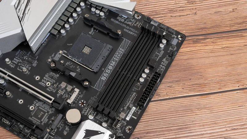
Advantages of PoP Technique:
1. Saving Space: Significantly improve the utilization rate of space, a key technology for miniaturization of mobile devices (phones, tablets).
2. Improve Performance: The interconnect paths between the top and bottom layer chips are extremely short (typically <1mm), reducing signal latency and power consumption, and increasing transmission bandwidth.
3. Design Flexibility: Allows for the combination of processors and memory from different manufacturers, facilitating product iteration and configuration selection.
4. Reduce Cost: Compare to integrating two chips into the same package (such as some forms of SiP), PoP could utilize standardized packaging and testing processes.
Core Process Steps of PoP Assembly:
The challenge of PoP assembly lies in completing the reflow soldering of all interconnect points in one operation: the top and bottom packages, and the bottom package with the PCB. It requires precise management of material, equipment and assembly process.
The entire process is mainly divided into the following key stages:
1. Solder Printing
● Bottom PCB: Print the solder on the main circuit board where the PoP locates, to solder the BGA's bottom solder balls on the bottom package.
● Top Package: Solder is applied to the pads on top of the bottom package. This is the key point of the PoP assembly process. There are two main methods:
* Pre-applied Solder Paste Method: Using micro-stencils or jet printing technology, tiny solder paste dots are precisely printed on the top pads of the bottom package.
* Ball Placement Method: Tiny solder balls are pre-placed on the top pads of the bottom package. This method offers good consistency and is currently the mainstream, especially for fine-pitch PoP.
2. Component Placement
This is a high-precision two-step placement process:
Step 1: Place the bottom package. The bottom chip (e.g., processor) is mounted by aligning its bottom BGA solder balls with the solder paste on the PCB.
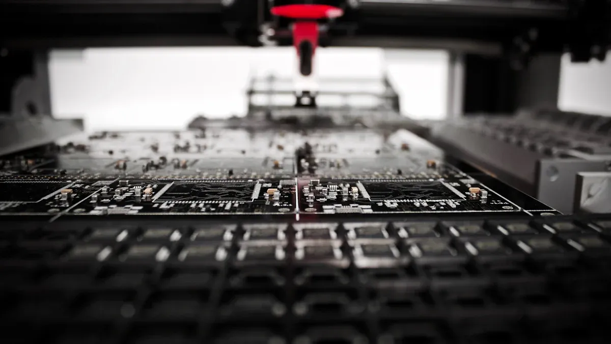
Step 2: Mount the top package. following step 1, within the same production cycle, mount the top chip (e.g., memory) by aligning its bottom solder balls or pads with the top solder of the bottom package which is already placed on the PCB. This requires extremely high precision and stability from the pick-and-place equipment, typically using a double-cantilever or specialized multi-functional mounting head.
3. Reflow Soldering
● The mounted stack of chips (top layer + bottom layer) and the PCB enter the reflow oven.
● In a hot air or vacuum reflow oven, the solder at all connection points (solder paste on the PCB, and solder between the top and bottom layers) melts simultaneously.
● In the melting state, relying on the surface tension and gravity of the solder, solder joints are formed, achieving electrical and mechanical connections.
● This is the most critical process: the temperature profile must be precisely controlled, to ensure that each solder joints achieves a good condition and that the chips are not damaged by thermal stress.
4. Inspection and Testing
● Automated Optical Inspection: to check the alignment of components after soldering.
● X-ray Inspection: Since solder joints are covered under the package, 2D/3D X-rays must be applied to inspect the quality of BGA solder joints and PoP innerlayer solder joints, such as bridging, cold solder joints, and voids.
● Electrical Testing: Confirms that the stacked chips function correctly.
Key Challenges and Solutions of PoP Assembly
| Challenges | Description | Solution |
| Alignment Accuracy | The solderpads on the top package and bottom package are very small, so as the space, which requires extremely high alignment accuracy (typically ±0.05mm). | Use high-precision pick-and-place equipment and vision alignment systems, and ensure the coplanarity of the packages and the consistency of solder balls. |
| Solder Amount Control | The amount of solder between packages must be precise. Too much solder leads to bridging, too little leads to cold solder joints. | Use ball placement instead of printed solder paste; Control the ball size and solder paste amount precisely. |
| Solder Yield | Single-pass reflow creates multiple rows of invisible solder joints, increasing yield risk compared to single-layer BGAs. | Optimize reflow temperature profiles (typically using a "tent-shaped" profile), use nitrogen protection to reduce oxidation, and employ vacuum reflow to reduce voids. |
| Stack Height | Total height needs strict control to meet thin and lightweight product requirements. | Use ultra-thin packages, low-radius molding compounds, and smaller solder balls. |
| Thermal and Stress | High thermal density after stacking, coupled with varying coefficients of thermal expansion of different materials, could generate thermal stress. | Consider heat dissipation in PCB and package design; Use underfill to enhance mechanical strength and thermal fatigue resistance. |
Variation of Assembly Process: Underfill
For applications with extremely high reliability requirements (such as automotive electronics), after PoP assembly, underfill is applied between the bottom package and the PCB, and sometimes even between the top and bottom packages. The adhesive penetrates the solder ball gaps through capillary action, and after curing, it significantly absorbs mechanical stress (such as impact and bending), improving thermal fatigue life caused by temperature cycling.
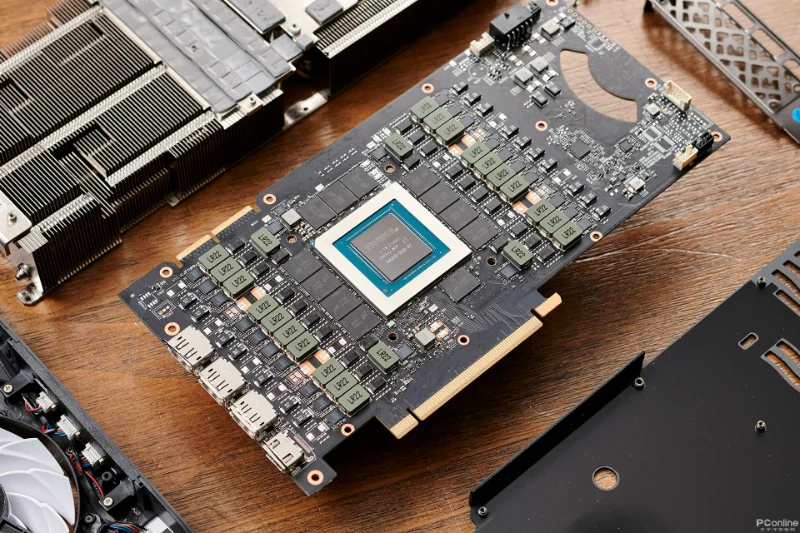
In summary, PoP (PoS) assembly is one of the advanced techniques of modern high-density electronic assembly. The core elements of a sucessful PoP assembly are:
● Materials: High-performance solder balls, solder paste, and substrates.
● Equipment: High-precision pick-and-place machines and controllable reflow ovens.
● Process Control: Precise management of the entire process, from solder paste/ball placement to mounting and reflow.
● Inspection: Powerful non-destructive testing capabilities such as X-ray.
As the number of chip I/Os increases and pitch minimization at sametime, PoP technique is also evolving forth to finer pitches (e.g., 0.35mm pitch) and higher stacking layers (e.g., PoPoP), continuously drive the evolution of electronic devices to smaller, faster, and more powerful designs.
Benlida is a professional PCB manufacturer and provides PCB assembly service for 14 years, if you are working through PoP assembly for your PCB&PCBA, you are welcome to contact Benlida to get a clue for how to proceed for manufacturing!
Benlida is at your service!

 en
en


 WhatsApp